big_fudge98
Member level 2
Hi,
I am trying a microstrip transmission line simulation in HFSS. I imported the GDS file, and setup the ports. I am using HFSS simulator (not Planar EM) and Phi Meshing. However, I see my results changing with horizontal padding.
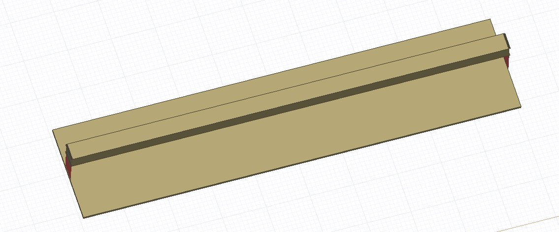
The following is my transmission line. I am designing it for a SiGe IC.

With the default dielectric horizontal padding (0.005) option, my results are :

With dielectric horizontal padding of 0.05, my results are :

With dielectric horizontal padding of 0.5, my results are :

It can be observed that phase of S21 changed by more than 5 degrees. Is this expected? Does anyone know why this would have happened? Or do you think I am setting up the simulator wrong? (I am new to HFSS 3D layout).
I am trying a microstrip transmission line simulation in HFSS. I imported the GDS file, and setup the ports. I am using HFSS simulator (not Planar EM) and Phi Meshing. However, I see my results changing with horizontal padding.
The following is my transmission line. I am designing it for a SiGe IC.
With the default dielectric horizontal padding (0.005) option, my results are :
With dielectric horizontal padding of 0.05, my results are :
With dielectric horizontal padding of 0.5, my results are :
It can be observed that phase of S21 changed by more than 5 degrees. Is this expected? Does anyone know why this would have happened? Or do you think I am setting up the simulator wrong? (I am new to HFSS 3D layout).