Continue to Site

Welcome to EDAboard.com

Welcome to our site! EDAboard.com is an international Electronics Discussion Forum focused on EDA software, circuits, schematics, books, theory, papers, asic, pld, 8051, DSP, Network, RF, Analog Design, PCB, Service Manuals... and a whole lot more! To participate you need to register. Registration is free. Click here to register now.

TQFP 44 Land Pattern?

Status
Not open for further replies.

mImoto

Full Member level 4
Joined
Feb 21, 2002
Messages
210
Helped
4
Reputation
8
Reaction score
1
Trophy points
1,298
Activity points
1,733
tqfp44 footprint

Hello,

I am going a bit crazy looking for a good land pattern for the TQFP 44 pins package (PIC18f448). Any link where I can find it or information about how to design a Land pattern. I am junior with footprints design.

Thanks a lot and best regards,

mimoto
 

tqfp44 land pattern

Examples of TQFP44 land pattern:
 
tqfp footprint

**broken link removed**
 

tqfp44

mImoto said:
Hello,

I am going a bit crazy looking for a good land pattern for the TQFP 44 pins package (PIC18f448). Any link where I can find it or information about how to design a Land pattern. I am junior with footprints design.

Thanks a lot and best regards,

mimoto

What s/w will you use the land pattern in, Orcad, Pads, Protel.......if you let us know someone can let you know if it already exists in the library or how to make it.

The dimensions for the land pattern for your PIC18F448 are on page 383 of the data sheet

**broken link removed**

:R
 

tqfp 44 land pattern

Hi,

thanks for the info. About the info of the datasheet I have look again and it is the size of the package but it is not in my opinion the size of the land pattern. The others are what I have been looking for.

thanks a lot and best regards,

mimoto
 

qfp 44 footprint

mImoto said:
Hi,

thanks for the info. About the info of the datasheet I have look again and it is the size of the package but it is not in my opinion the size of the land pattern. The others are what I have been looking for.

thanks a lot and best regards,

mimoto

mImoto,

Cool, you got what you needed, but I am confused.

All dimensions on the PIC data sheet are there for the land pattern, max/min tolernaces, pitch, pin dimensions and everything.

There is a lot more to a land pattern than just the pad sizes like placement tolerances, paste->pad size->pin size->paste volume calculations and so on. Using an off the shelf footprint is not always good as it does not know your process parameters.

Just getting the pad size from a ready made footprint is not always the answer when you want to factor in manufacturing yeild & DFM.

:R
 

Hi..
This is Nithin. Could anybody get me the TQFP for CC2530 IC which having 40pins with 1 Termal pad at the center. So totally 41Pads. pls sent me for Orcad Library..

Thanks a Lot.. frnds.

-Nithin
 

i'm finding it difficult to build land pattern of TQFP-44 (PIC16F887)
16_1316820694.jpg


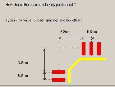
getting that relative distance for pins correct is being hit&miss;
the 3.8mm in the pic
should it be 2mm ? the package width is 10mm, the overall width 12mm....
and I don't see the Microchip spec giving that distance specifically.

anyone got this land pattern for protel they can share?
need a TQFP-64 also


(hmm..is there a edaboard problem? this post is not showing up on "New Posts")
 

Attachments

  • tqfp44 relative.jpg
    tqfp44 relative.jpg
    10 KB · Views: 112
Last edited:

If you are using a good PCB layout software, you should be able to draw any land patterns yourself with the mm/inch deatils given on the datasheet of the componenet.
Cheers
 

you should be able to draw any land patterns yourself with the mm/inch deatils given on the datasheet of the component.
xaccto is asking how the pad distance should be selected according to package dimensions.
Why do you think that they are any different from the standard TQFP44.
What's the standard footprint? It doesn't exist. For the 10 mm body TQFP package, you'll find suggestions of pad center distances between 11.4 mm (Microchip PIC18F2480 DS), 11.6 mm (the said ST datasheet) and about 12 mm (IPC conformant Altium Designer footprint library). 11. 4 mm can be calculated according to the simple rule, that a nominal length (0.6 mm) foot should be centered to the pad. This rule can be found e.g. in https://home.jeita.or.jp/tsc/std-pdf/EDR-7311A.pdf

IPC is in contrast suggesting an asymmetrical pad placement with more free pad length on the outer side. I'm not sure about the objectives of the IPC footprint, but as a side effect, they are good for hand soldering.
 

Ipc-7351
!!!!!!!!!!!!!!!!!!!!!!!!!!!!!!!!!!!!!!!!!!!!!!!!!!!!!!!!!!!!!!!!!!!!!!
 

Status
Not open for further replies.

Part and Inventory Search

Welcome to EDABoard.com

Sponsor

Back
Top