Continue to Site

Welcome to EDAboard.com

Welcome to our site! EDAboard.com is an international Electronics Discussion Forum focused on EDA software, circuits, schematics, books, theory, papers, asic, pld, 8051, DSP, Network, RF, Analog Design, PCB, Service Manuals... and a whole lot more! To participate you need to register. Registration is free. Click here to register now.

[SOLVED] Totem-pole input resistor value

Status
Not open for further replies.

mrinalmani

Advanced Member level 1
Joined
Oct 7, 2011
Messages
463
Helped
60
Reputation
121
Reaction score
58
Trophy points
1,318
Location
Delhi, India
Activity points
5,285
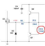
I am attaching a schematic below. The question is... do we actually require the PNP input resistor (R10) to limit the base current during MOSFET turn off?
The BJTs have a peak base limit of 1A each.
I had added R10 for safety. However since the input of both the BJTs is internally connected in a standard Totem-pole IC, it is not possible to add R10. Another question would be... is adding the base resistor a standard practice? If not, will it not result in a surge current through the base?
Please help
 

Attachments

  • Capture3.PNG
    Capture3.PNG
    14.3 KB · Views: 263

You already have R9 for current limiting. I don't see a purpose of R10 at all. I would also chose a lower value for R12 (depending on the available driver current), because it helps to pull down the gate voltage below +0.7 V and up to full driver voltage.

For large gate capacitance values, transistors with higher rated collector current (and particularly higher current gain at medium currents) are preferred. There are nice devices like ZXTP2025F and ZXTN2031F. A 1A transistor will be most likely self limiting by low current gain above 1 A, exceeding 1A for a few 10 ns won't be a big problem otherwise.

If asymmetrical gate currents are intended, you'll use RD circuits in place of R9. Usually, you rather want slower turn-on than slower turn-off.
 

The limiting Resistor R9 is only 5 ohm. I am not much concerned about the collector current, firstly coz the collector limit is 2A and secondly secondly as you said, due to the low gain at high current.
What is bothering me is the base current. When the base is pulled down, there is free path through the emitter-base junction (acting as a diode). Now there are two parallel paths.
1. Through emitter-collector-ground
2. Through emitter-base-ground
What ratio will flow in the two paths? The second path is acting simply as a diode. Will the gain formula still hold?
Taking the NPN analogy, the equivalent circuit should be as attached below.

- - - Updated - - -

How do find the base current? Does the gain formula still hold. (Consider that the base-emitter is simply a diode, in parallel with another diode, ie, collector-emitter)
 

Attachments

  • Capture4.PNG
    Capture4.PNG
    3.4 KB · Views: 91
Last edited:

I guess it's acting like a regular transistor connection.. because when the base current rises enough to turn on the transistor, the collector current will surpass the (smaller) base current (it's a negative feedback). Higher the base current, (much) higher the colector current (proportional to the transistor gain ratio).

If there was only the base connected, it was acting like a simple diode indeed.
 

In this situation, both the paths are equally free. If collector is freely conductive, then so is the base path. Both equally conductive path in parallel!

- - - Updated - - -

Ok wait! Let me carry out a simulation. I'll post the results...

- - - Updated - - -

Capture5.PNG
It seems you are right. The paths are not equally conductive.
Thanks anyway.
 

The collector-emitter has a much lower impedance (reverse proportional with the collector current).
 

Unfortunately neither the transistor type nor the driver current has been mentioned. But any transistor that might be used in this circuit has still some current gain at rated current. The other interesting parameter is saturation voltage. Assuming Vbe = Vce as in your simulation is rather unrealistic because the driver will also contribute a certain voltage drop and the transistor won't be in saturation. So it's effectively impossible to exceed rated base current before rated collector current.

My previous comment about low current gain at high currents is relevant for those cases where the driver isn't able to provide sufficient base current, so the current gain is effectively the limiting parameter for achievable gate current.
 
"So it's effectively impossible to exceed rated base current before rated collector current."

Seems absolutely correct. Thanks!
 

Status
Not open for further replies.

Similar threads

Part and Inventory Search

Welcome to EDABoard.com

Sponsor

Back
Top