fareen
Full Member level 3
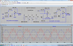
shoudnt it be Vo/Vs=g1*g2Without feedback
Vo/Vs = G2
because we have cascaded two amplifer and ignoring the noize signal taking the assumption Vn<<<VS
Follow along with the video below to see how to install our site as a web app on your home screen.
Note: This feature may not be available in some browsers.
shoudnt it be Vo/Vs=g1*g2Without feedback
Vo/Vs = G2
yes you are rightand the s/n is increased 56.23 times...
")
Now it is 50 when R21=5K :wink:using R21 5k does not give 50 gain of the amplifier but 100??
what exactly did i miss??Did you notice what you have missed in your gain formula? I guess you did