Continue to Site

Welcome to EDAboard.com

Welcome to our site! EDAboard.com is an international Electronics Discussion Forum focused on EDA software, circuits, schematics, books, theory, papers, asic, pld, 8051, DSP, Network, RF, Analog Design, PCB, Service Manuals... and a whole lot more! To participate you need to register. Registration is free. Click here to register now.

TL494 variable duty cycle

Status
Not open for further replies.

LIC33

Newbie level 4
Joined
Sep 28, 2021
Messages
6
Helped
0
Reputation
0
Reaction score
0
Trophy points
1
Activity points
78
The idea is to make a small push-pull converter and to introduce exact frequency and amplitude ripple in its output in order to test some voltage ripple sensitive circuitry that I'm developing.

I have thought that TL494 might be a good choice because of its two error amplifiers that should be able to control duty cycle.
I'm aware that I could use DTC to control duty cycle indirectly. I'm also aware that I can directly provide modulation signal to the FB pin.
However, I have to use some sort of feedback from the output to achieve exact DC offset and ripple as I need.

I have read the datasheet and it seemed obvious that I could simply provide input of the error amplifier with the proper DC offset with sine wave of desired amplitude from function generator and provide simple voltage feedback from the output scaled down with the resistor divider.

Since I currently I don't have any TL494 laying around and I have to wait for the delivery I decided to first simulate the simplest circuit in Micro-Cap as a proof of concept.
However, what should have been simple became a toil because instead of variable duty cycle what I get at the output is a sort of fixed frequency, fixed duty cycle burst mode.
I became curious so I have tested the PSpice model with the first schematic (boost converter) that I found on the net and the model seems to be working correctly.

At this point I simplified the proof of concept circuit to minimum in order to at least achieve some basic duty cycle modulation but with no luck.

The circuit is currently set in push-pull configuration.
Dead time is minimal and one error amplifier is set to maximal output because according to the datasheet the amplifier demanding the minimum pulse out dominates.
It seems logical to me that providing the second error amplifier with fixed voltage and with modulated signal should produce variable duty cycle.
However, what I observe on the outputs is indeed a minimal dead time but with fixed duty cycle output bursts.

While I could perhaps use that signal to drive push-pull transformer and produce desired modulated signal at the output of the entire device I'm quite curious as to what exactly I'm overlooking. It is most likely some obvious detail but for the moment I don't see what it is.

So, could someone please take a look at the schematic and the simulation results and perhaps point the mistake?
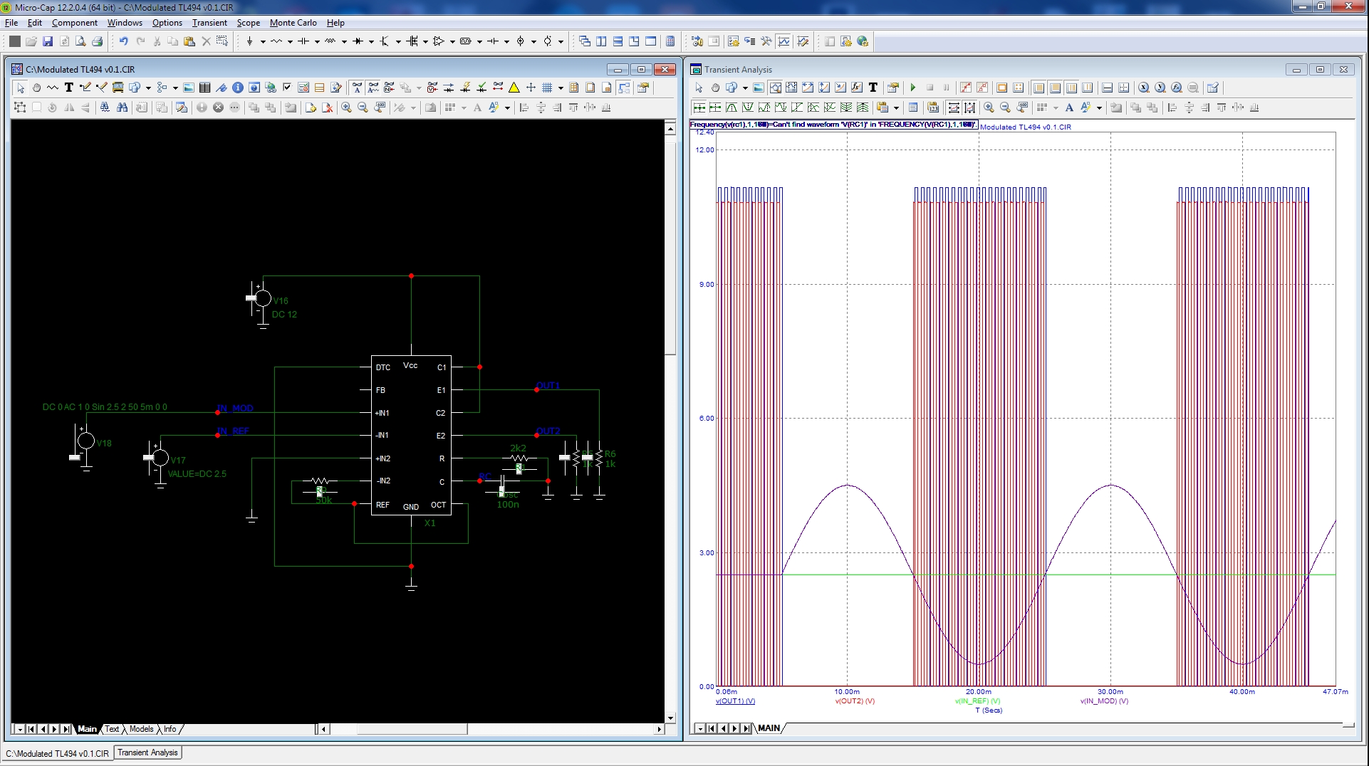
Modulated TL494 v0.1.jpg
 

What is range of freq you want ? Modulation and Unmod freq input.
Also modulation, any specifics like waveshape ?

Of course a combination of two VCOs and an analog multiplier would do....

Possibly LM331 VCO and modulate its control loop with multiplier -


Or use mixed signal part with DACs and A/D, latter to establish desired freq and amplitude
from setting pots, and tight code loop to do the mod calculation and DMA to move it to what
in effect would be a multiplying DAC....But latency to a step change in freq and amplitude request
a possible issue.


Regards, Dana.
--- Updated ---

Third possibility is a mixed sig part to gen analog mod and main waveforms, arbitrary or
sine or whatever, an A./D to read settings pots, And external analog multiplier to yield
the composite wave form. This would be two parts.

Regards, Dana.
 
Last edited:

This sim is just test of basic concept. In reality oscillator frequency will most likely be around 100 kHz to get around 50 kHz at the transformer (push-pull configuration). Modulation frequency will go up to 1 kHz, so simple small RC LPF should be adequate considering the light load at the output.

To me everything appears well within TL494 specifications.
 

Hi

I had a look at this Manufacturer's TL494 datasheet , and not understanding this kind of device much, I must say that your simulation set up is very different to the typical application on page 13. You said what you said about 'I have to use some sort of feedback from the output to achieve exact DC offset and ripple as I need' which in my ignorance is what IN1+ is for, isn't it? No chance of using a normal set-up and tweaking at the edges, instead...?

I'm certain you know that it's an internal comparator that controls PWM stuff based on signals received from EAs. Looking at your control signal into EA IN1+, by any small and remote chance are you confusing what the EAs do to the comparator input with the ripple you expect to see at the feedback voltage divider? Page 12 says: 'The output pulse width varies from 97% of the period to 0 as the voltage present at the error amplifier output varies from 0.5 V to 3.5 V, respectively.' while page 10 and the functional block diagram shows the internal PWM comparator.

As I won't have much to offer by way of a solution to your problem, a suggestion would be to start with a known functional schematic/cirrcuit and take back-steps one at a time from there with regard to modifying it to your requirements. Sorry I can't be of more help.
 

I'm certain you know that it's an internal comparator that controls PWM stuff based on signals received from EAs. Looking at your control signal into EA IN1+, by any small and remote chance are you confusing what the EAs do to the comparator input with the ripple you expect to see at the feedback voltage divider? Page 12 says: 'The output pulse width varies from 97% of the period to 0 as the voltage present at the error amplifier output varies from 0.5 V to 3.5 V, respectively.' while page 10 and the functional block diagram shows the internal PWM comparator.

You just may be right regarding the input signals that I've used may behave unexpectdely when the resulting voltage of the error amplifier was <0.5 V but the circuit behaved strangely even when it was not the case.

I took your advice (thank you for the reminder) and made a basic test setup as depicted in the datasheet.
Now I wonder if the TL494 model that I'm using is entirely correctly modeled because I was surprised to observe negative voltage appearing on the FB pin. It seems that I incorrectly assumed that this model is entirely equivalent to the physical device because people are using it successfully for many years. I suspect that the model may work correctly in most cases but perhaps not everything is modeled exactly identical to the physical device and with the unusal stimulus it may behave unpredictably.

I may be mistaken but negative voltage simply cannot appear at the FB pin of any physical TL494 device.
I guess that it would be best for me to wait for the physical device to arrive in order to test it on the bench and see how it compares with the simulated model.

Thank you again for reminding me to first try the most basic setup depicted in the datasheet.
 

Perhaps you should describe the ideal output / end result you are seeking - this will help inform all other responses.

As it has two error amps - one can be set up for peak current limiting - very useful for protection

the other can be set up such that you can modulate the output based on a feedback loop - if the output needs to be isolated - then usually an opto can be incorporated to do this and the error amp then becomes a voltage follower.

Good luck.
 

Perhaps you should describe the ideal output / end result you are seeking - this will help inform all other responses.

As it has two error amps - one can be set up for peak current limiting - very useful for protection

the other can be set up such that you can modulate the output based on a feedback loop - if the output needs to be isolated - then usually an opto can be incorporated to do this and the error amp then becomes a voltage follower.
I'm aware that TL494 have two error amps and I chose it exactly for the reasons that you've mentioned.

As far as the purpose, on the output of the device I need DC (500-3500 V) with controlled ripple added on top of it.
To be more precise, I need adjustable positive DC at the output (500-3500 V) as well as adjustable ripple amplitude (usually ~5% of DC voltage) and frequency (1-1000 Hz sine). Modulation signal is provided by MCU and 10-bit DAC (already wrote and tested firmware for it).

It seems to me that the most convenient and simplest way to do that is to simply use push-pull transformer with bridge rectifier and LC low pass filter at its output. Loads under test are quite light (high impedance, very low current 1-2 mA) so the resistor divider used for feedback loop is also serving to reduce total load impedance in order to increase usable bandwidth of the ripple up to 1000 Hz. Sine wave shape of the added ripple is not ideal in such configurations but it's suitable enough for my purposes.

ATM my problem is that the sim model acts strangely so it seems that I'll need to wait for the physical device to arrive and test this modulation scheme in hardware.

The alternative to that is using more conventional analogue to PWM converter with triangle wave generator and fast comparators. Then all that remains is feeding PWM signal into some half-bridge driver which will provide internal flip-flop, MOSFET drivers and dead-time control. Additional comparator to primary current may be used for latched shut down of half-bridge driver. I'm pretty sure that it would work better than TL494 but if I have to reduce number of components if possible because the rest of the circuitry in which this will be used is quite complex and takes a lot of space in a small enclosure.

That's why I was thinking that voltage mode PWM controller such as TL494 may address all of that (sawtooth generator, two error amplifiers available to control duty cycle, dead-time control and somewhat capable output drivers) in a single package and with minimal additional components.
 

Future reference if you need a part that typically results in single chip solutions this all onchip -

1632962221512.jpeg


There is a set of community libraries that can also be used with stuff like DDS, CPLD, MAC, 74HC
equivalents.........

Regards, Dana.
 

Yes but you need a slower feedback loop to set the AVERAGE DC level out, and then another form of modulation control to create the AC on top of the average DC,

not as straight forward as you might have first thought,

alternatively, as you say, you can create a demand signal that has the AC + DC in one signal and then PWM modulate a push pull to generate the required output,

if the load is only a few mA - you can RC filter the o/p rather than LC, which creates mores poles that need compensation in the feedback loop
 

@danadakk
Thank you for the info but I don't have any experience or development tools to use FPGA.
8 and 16 bit microcontrollers are usually suitable enough for my requirements.


@Easy peasy
Thank you for the RC filtering advice.
The truth is that I have a few high voltage chokes laying around but no high voltage resistors and I wanted to avoid making long chains of normally available resistors (usually they're rated up to 300V only).
I will take account what you've said regarding compensation.
 

Status
Not open for further replies.

Similar threads

Part and Inventory Search

Welcome to EDABoard.com

Sponsor

Back
Top