Continue to Site

Welcome to EDAboard.com

Welcome to our site! EDAboard.com is an international Electronics Discussion Forum focused on EDA software, circuits, schematics, books, theory, papers, asic, pld, 8051, DSP, Network, RF, Analog Design, PCB, Service Manuals... and a whole lot more! To participate you need to register. Registration is free. Click here to register now.

TL494 Push Pull Modified Sinewave Inverter simulation problem

Status
Not open for further replies.

sraheja

Newbie level 4
Joined
Jun 19, 2010
Messages
6
Helped
0
Reputation
0
Reaction score
0
Trophy points
1,281
Location
Kanpur, India
Activity points
1,350
I am trying simulate a modified sine wave inverter (12V to 220 V output/ 200 Watts output) based on push pull topoplogy using TL494 in LTSpice. The TL494 oscillator is being driven for a 50Hz push pull frequency.

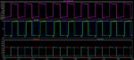
In order to create a three level voltage output, I am trying to use the dead time control feature of TL494. This has been set using resistors R14 and R15 in the attached circuit. While the output from TL494 looks OK (the dead time is clearly seen in the waveform for the totem pole output driving the mosfet gates), the voltage wave forms at the primary and secondary of the push pull transformer are not showing zero output voltage during the dead time. The voltages directly swing from -240V to +240 V, without staying at 0V level. Is it wrong to expect that during the dead time when both mosfets are off, the voltage output at the transformer secondary should also come to zero.
If however I significantly increase the load, say by reducing the load resistor R17 from 200E to 2E, I do get a modified sine wave out put but with much lower voltages (may be due to resistive voltage drops). Can some one please comment as to what might be happening in the simulation and whether the same would also be expected in the real circuit?

thanks in advance,
 

Attachments

  • TL494 Inverter Circuit Diagram.pdf
    17.8 KB · Views: 248
  • Simulation Waveforms.jpg
    Simulation Waveforms.jpg
    155.7 KB · Views: 213

It is the same in real life. When you put current through a coil you charge it with energy. If you don't discharge the energy it stays in the coil. When you connect resistor to the coil it discharges the the energy, the lower the resistor the faster the discharge.
Soon you will get mathematical explanations from the better educated experts.
 
For tri-level voltage source, did you consider tri level drivers for +,0,- rather than +, tri-state,- ? What are the magnetics properties for primary L and coupling factor?

Are you using not planning on using PWM?
 

modified sine wave

This has a dead time which is 0V.

There are two ways of thinking about it: (a) The output might go to 0V in the sense that everything goes to high impedance, or (b) it might go to 0V in the sense of providing a low-impedance path to 0V ground.

Which is your circuit doing? I believe you want to create a path to 0V ground. This is particularly important if current flow needs to continue through any component during dead time. Example, if your load is something other than ohmic resistance, or if your supply current waveform is not aligned with the supply voltage waveform.
 

Thanks all, for giving insights. I went further on the suggestion given by Vbase that the simulation results are in order. But I had naively, thought that push pull transformers did not store energy but just transferred it.

With the same load, I have re-simulated with a changed transformer. The primary side inductance are increased to 50mH (for L1 and L2) and the secondary side inductances are increased to 5H (for L3 and L4). Intuitively these look impractical to me. This now gives an improved waveform at the output (see https://obrazki.elektroda.pl/8567135200_1430814946.jpg)

My hopes of designing a modified sine wave inverter with a single push pull stage are now dwindling. An H bridge driver on a high voltage DC bus looks like a superior (though complex) solution as the time for which the output remains at zero voltage would now be independent of the magnitude of the load.

If somebody has better ideas of making a modified sinewave inverter with TL494/ SG3525 or any such type of PWM Controller ICs in a single push pull stage, then the same would be appreciated.
 

This has a dead time which is 0V.

I could not understand the 0V part. I am getting dead time in output (not exactly zero but a low voltage level) only when the load is too high or I use very high inductance values for the transformer.

And yes, I do intend to have a path to ground so that current flow happens during the dead time for non resistive loads. I had not thought in these terms before.

My circuit intends to work like an inverter for both resistive and non resistive loads (12V DC to 220V AC, 50Hz, 200 Watts of power output)
 

As you already found out in your simulation, the square wave output is driven by the transformer inductance.

I don't understand how you arrived at the transformer inductance values, but they are considerably below the expectable main inductance of standard 50 Hz transformers. To get an exact "three-level" waveform, you would need a power stage that can source and sink reactive current. The transformer push-pull stage can't.
 
I don't understand how you arrived at the transformer inductance values, but they are considerably below the expectable main inductance of standard 50 Hz transformers.

This is exactly the sort of advice I am looking for and you have to excuse me for my inexperience. I can say that even with the increased inductance values as I have tried the trilevel voltage state is still not perfect. To improve it further i need to further increase the inductance. When browsing through resources available on the internet, we get more information on inductance values for high frequency SMPS transformers and very little information in terms of inductance for 50Hz transformers. Would you have some data readily available for typical inductance values and winding information for 50Hz push pull transformers in 100 Watt to 500 Watt power range or how to arrive at the same? In my simulation i have used the hit and trial method. Kept increasing the inductance till I got a wave form that looked OK. Practically, I tried to work with some salvaged transformers from old inverters. They happened to have lower inductance when measured on an LCR meter and I landed up bursting my mosfets due to overcurrent. So before taking to breadboarding this time and buying out new transformers, I wanted to do a reasonable simulation to make sure that they worked well for a modified sine wave design.

To get an exact "three-level" waveform, you would need a power stage that can source and sink reactive current. The transformer push-pull stage can't.

Could you elaborate this a little further. What type of power stage topology is then next (in increasing order of complexity) more suitable? Do you have a sample circuit block/diagram. The functional target is to design a low cost inverter which works well with inductive loads like ceiling fans (no audible humming sound is the criteria) .
 

What type of a driver do you propose for +, 0 and -. The +, midlevels, and - (the middle level voltage is not zero but depends on transformer and magnitude/type of load).

I do plan on using the PWM, but just that I wanted to involve load/line regulation later when the basic concept with respect to typical transformer design and waveform had worked out in the simulation. I do not believe that lack of PWM control is the culprit here. I am pushing the design to work at maximum duty level, with minimum dead time it is configured for.
 

To give a brief answer, a H-bridge would be able to force the output voltage despite of a reactive current, if the transistors are controlled for synchronous switching.

The other question is if you actually need to reproduce a predefined voltage waveform with your inverter, or if you can accept a deviation at low loads.
 

    V

    Points: 2
    Helpful Answer Positive Rating
I agree with FvM

I also believe for high power 3 phase bridge drivers for high efficiency single phase is best for apps >>100W resulting in low dynamic losses.

If you can limit the load swings 2 phase half bridge (with ventre tap making a full bridge) can work. But if not , well then valley sensing on current to commutate is better. Recall time constant of valley will be L/R related. for variable load R. Any load capacitance will cause resonance; which may result in audible noise of inverter if driving a laptop charger.

Quasi Synchronous resonant Chips are designed to support this with higher rates and thus more compatible with cost-effective ferrite transformers, rather than iron core.
 
  • Like
Reactions: sraheja

    V

    Points: 2
    Helpful Answer Positive Rating

    sraheja

    Points: 2
    Helpful Answer Positive Rating
Status
Not open for further replies.

Similar threads

Part and Inventory Search

Welcome to EDABoard.com

Sponsor

Back
Top