Continue to Site

Welcome to EDAboard.com

Welcome to our site! EDAboard.com is an international Electronics Discussion Forum focused on EDA software, circuits, schematics, books, theory, papers, asic, pld, 8051, DSP, Network, RF, Analog Design, PCB, Service Manuals... and a whole lot more! To participate you need to register. Registration is free. Click here to register now.

Timer Circuit Using Transistor

Status
Not open for further replies.

gauravkothari23

Advanced Member level 2
Joined
Mar 21, 2015
Messages
640
Helped
5
Reputation
10
Reaction score
4
Trophy points
1,298
Activity points
6,922
Hi All.
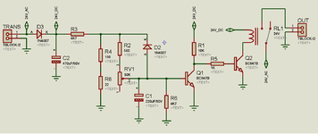
I have built a timer circuit using Transistor. (Circuit Diagram Attached)
The power source is 24V 3 Amps Transformer. and i am operating a 24V 10 RPM AC Motor for one of my application.
On Power ON, The motor will be ON for a specific period of time and the time is decided by C1 Capacitor and R2 and RV1 Resistor. as soon as the voltage at transistor base Q1 is close to 0.7V, the transistor goes ON and motor goes OFF. To restart the motor, the Mains power has to be switched OFF and ON Again.
R4 and R8 are used with D2 diode to discharge the power left in C1 after Mains are switched OFF.

what my problem is, suppose at first power ON, the motor stays ON for 5 Seconds. Later when the mains are put to OFF and ON again, the motor goes OFF in hardly 2 seconds, because of C1 capacitor which stays charged. Have noticed that the capacitor C1 takes around 8 to 10 seconds for complete discharge. so in such case, i cannot Restart the Motor for next 10 to 12 seconds and have to wait for capacitor to get discharge.

How can i discharge the Capacitor C1 fast say within 2 seconds.

Putting the mains OFF and ON is the only option what i have to provide to restart the motor.
 

Attachments

  • Timer Using Trans.png
    Timer Using Trans.png
    39.2 KB · Views: 149

Solution
Your problem is not C1, it’s C2. C1 will discharge through D2, R4 and R8, but the discharge path for C2 is through that big R2. You need a low resistance discharge path for C2. Does it really need to be 470uF?
Hi,

when powered ON for a while the voltage at C1 becomes saturated. Maybe at about 0.7V. It is limited by V_BE of Q1.

Now you want the capacitor to be discharged by D2. But it has a similar forward voltage than V_BE, thus the discharge process fails.
It mainly discharges via R2.

*****
There are several solutions.

1) A simple solution is to use a schottky diode in place of D2. This give not the perfect improvement.


2) One could be to charge C1 to a much higher voltage.
maybe add a zener between C1 and Q1

Klaus
 

Your problem is not C1, it’s C2. C1 will discharge through D2, R4 and R8, but the discharge path for C2 is through that big R2. You need a low resistance discharge path for C2. Does it really need to be 470uF?
 

Solution
Hi,

when powered ON for a while the voltage at C1 becomes saturated. Maybe at about 0.7V. It is limited by V_BE of Q1.

Now you want the capacitor to be discharged by D2. But it has a similar forward voltage than V_BE, thus the discharge process fails.
It mainly discharges via R2.

*****
There are several solutions.

1) A simple solution is to use a schottky diode in place of D2. This give not the perfect improvement.

Klaus
I tried using a schottky, but its was not a reliable solution.
2) One could be to charge C1 to a much higher voltage.
maybe add a zener between C1 and Q1
Yes, i Think i should try this, adding a 3.3V or 4.7V Zener Diode. where again 1N4007 will help me out for faster discharge, atleast till 0.7V
--- Updated ---

Your problem is not C1, it’s C2. C1 will discharge through D2, R4 and R8, but the discharge path for C2 is through that big R2. You need a low resistance discharge path for C2. Does it really need to be 470uF?
My problem is C1, because its the only capacitor which stays charge.
C2 wont stay charged for longer time because R3, R4, R8 is the only path where C2 would get discharge easily, it wont cross R2. Ofcourse R4 and R8 makes 172 Ohms. and R2 itself is 560 Ohms. and even if luckily it crosses R2, RV1, which is sometimes 50K, would block the path.
 
Last edited:

What is accuracy of timing over T and V and component variances you are seeking ?

Regards, Dana.
 

I tried using a schottky, but its was not a reliable solution.

Yes, i Think i should try this, adding a 3.3V or 4.7V Zener Diode. where again 1N4007 will help me out for faster discharge, atleast till 0.7V
--- Updated ---


My problem is C1, because its the only capacitor which stays charge.
C2 wont stay charged for longer time because R3, R4, R8 is the only path where C2 would get discharge easily, it wont cross R2. Ofcourse R4 and R8 makes 172 Ohms. and R2 itself is 560 Ohms. and even if luckily it crosses R2, RV1, which is sometimes 50K, would block the path.
No, C1 is not the the only capacitor that stays charged. Try running a simulation of this.

R3,R4, R8, C1 has a time constant of 2.2 seconds, thus, it will take about 10 seconds for C1 to completely discharge. The discharge path for C2 has a time constant of about 37milliseconds, but C1 is going to keep C2 charged.

And, yes, the diode drop of D2 will be a problem in that the base voltage of the transistor won't drop low enough.
 

Hi,

2) One could be to charge C1 to a much higher voltage.
maybe add a zener between C1 and Q1

Klaus
i am still facing a problem with adding a zener diode between Q1 base and C1.
have added 4K7 resistor to Base and Emitter (GND). so here when the mains are put to ON, voltage level on Q1 base reaches to 0.72V MAX. but as soon as the main as put to OFF, the voltage from 0.72V to 0.60V goes down very slowly which again takes aroung 6 to 7 seconds, and below 0.60V it decreases rapily say within MAX 1 Seconds.
i Also tried adding 4K7 Resistor across C1, but in such cases C1 does not gets charged. i tried increasing the resistor value too. but does not makes sense.
--- Updated ---

No, C1 is not the the only capacitor that stays charged. Try running a simulation of this.

R3,R4, R8, C1 has a time constant of 2.2 seconds, thus, it will take about 10 seconds for C1 to completely discharge. The discharge path for C2 has a time constant of about 37milliseconds, but C1 is going to keep C2 charged.

And, yes, the diode drop of D2 will be a problem in that the base voltage of the transistor won't drop low enough.
yes, i agree with you. but my problem is how can i discharge the C1 Cap easily as rapidly.
for C1 to charge C2, the only path which is available is through RV1, R2, and R3. but before R3, it will go through R4 and R8 Too. which has too dissipate C1 rapidly, but it does not.
 
Last edited:

Hi,

please show your current schematic.

have added 4K7 resistor to Base and Emitter (GND)
Why did you add one? R5 already was there.

as the main as put to OFF, the voltage from 0.72V to 0.60V goes down very slowly which again takes aroung 6 to 7 seconds
Yes, but with the 3V3 zener the threshod voltage at the capacitor is around 3.7V.
So when power is switched OFF the capacitor voltage - due to D2 - is rather fast down below 0.65V .

And when power is switched ON again it takes time for the capacitor to charge from 0.65V up to 3.7V
(before it discharged to 0.5V and switched ON at 0.65V ... or so.)

***

Again: a schottky diode will improve the discharge behaviour of C1.

****

Do you use a simulation tool? I recommend to do so.

Klaus
 

i am still facing a problem with adding a zener diode between Q1 base and C1.
have added 4K7 resistor to Base and Emitter (GND). so here when the mains are put to ON, voltage level on Q1 base reaches to 0.72V MAX. but as soon as the main as put to OFF, the voltage from 0.72V to 0.60V goes down very slowly which again takes aroung 6 to 7 seconds, and below 0.60V it decreases rapily say within MAX 1 Seconds.
i Also tried adding 4K7 Resistor across C1, but in such cases C1 does not gets charged. i tried increasing the resistor value too. but does not makes sense.
--- Updated ---


yes, i agree with you. but my problem is how can i discharge the C1 Cap easily as rapidly.
for C1 to charge C2, the only path which is available is through RV1, R2, and R3. but before R3, it will go through R4 and R8 Too. which has too dissipate C1 rapidly, but it does not.
After looking at this again, I realize this circuit is not working anywhere near close to how you THINK it's working.

AGAIN: C2 is what's controlling your timing, not C1. Maybe look into using a 555 timer?

And definitely do a simulation; it will be very helpful.
 

Hi,

Me too thinks that C1 is controlling the delay....

Klaus
Run a simulation if you’re not convinced. C2 gets charged to 24 volts when power is applied. When power is removed C2 discharges slowly through R3 (4.7K).

But, it's even worse: I don't think there's enough voltage to ever drive the base of Q1 on. There's a voltage divider of R3,R4,R8,R2,RV1,R6. With RV1 at minimum, there's about 0.73V. As RV1 is increased, presumably to increase the on-time, the voltage available will drop well below Vbe.
 

Hi,
When power is removed C2 discharges slowly through R3 (4.7K).
I have to admit, I indeed missed R3.
I completely ignored it, just wondered about the power dissipation in R4.

Thanks for clarifying this.

*********
With R3 = 4k7 the voltage at C2 never can rise to a voltage level that the zener (my recommendation) becomes conductive.

*********
Without R3 my recommendation should work, but the power dissipation is too high.

*********

Sorry for my mistake.

Klaus
--- Updated ---

Added:

My design recommendations (using most of the exisitng circuit)
and using the series 4V7 zener:

design/calculation back from Q1:
* Q1_VBE = 0.6V
* V_Zener = 4.7V
* ON threshold of C1 = 0.6V + 4.7V = 5.3V

since Tau is at 63% level, one could use the RC input voltage about 5.3V/0.63 = 8.4V (average)
(using this 63% makes the calculation for the expected ON delay more simple,
because it becomes 1 tau = (R2 + RV1) x C1)

C2 needs be be much smaller value d´to get dischrged rather fast..this also means there will be a voltage ripple due tothe half wave rectified AC input.

with 24V AC in I expect C2 to get charged to about 33V peak. --> because of ripple may be 30V average
so one needs a voltage divider 30V --> 8.4V

let´s R3 be 4k7, then R4 needs to be about 1800 Ohms.(Omit R8)

Now the total load at C2 is about 4k7 + 1k8 = 6k5

To get a fast dischrage maybe C1 = 15uF

.. I did not test this all. Let this be the OP´s job.

Klaus
 
Last edited:
Run a simulation if you’re not convinced. C2 gets charged to 24 volts when power is applied. When power is removed C2 discharges slowly through R3 (4.7K).

But, it's even worse: I don't think there's enough voltage to ever drive the base of Q1 on. There's a voltage divider of R3,R4,R8,R2,RV1,R6. With RV1 at minimum, there's about 0.73V. As RV1 is increased, presumably to increase the on-time, the voltage available will drop well below Vbe.
Yes Sir,
You were right. Actually C2 was the issue. with the same circuit i changed the value of C2 from 470uF to 10uF.
and R6 to 47K. Which made the system work perfect. Now the voltage at Q1 Base drops down rapidly within a millisecond when RV1 is at minimum and hardly 2 seconds when RV1 is at maximum.
Thanks.
I still don't believe it. First of all, with a 10uF cap, you're going to have a LOT of ripple on your 24VDC. Secondly, with RV1 at 50K, you'll have a maximum of about 400mV on the base of Q1. Are you sure your schematic shown in the original post reflects your actual circuit? Thirdly, the voltage at the base of Q1 should RISE, not fall.
 

I still don't believe it. First of all, with a 10uF cap, you're going to have a LOT of ripple on your 24VDC. Secondly, with RV1 at 50K, you'll have a maximum of about 400mV on the base of Q1. Are you sure your schematic shown in the original post reflects your actual circuit? Thirdly, the voltage at the base of Q1 should RISE, not fall.
Yes,
The PCB is exact same as the schematic posted.
The voltage at the Q1 Base rises when mains are ON, but drops rapidly as soon as mains switched OFF
 

Status
Not open for further replies.

Part and Inventory Search

Welcome to EDABoard.com

Sponsor

Back
Top