Continue to Site

Welcome to EDAboard.com

Welcome to our site! EDAboard.com is an international Electronics Discussion Forum focused on EDA software, circuits, schematics, books, theory, papers, asic, pld, 8051, DSP, Network, RF, Analog Design, PCB, Service Manuals... and a whole lot more! To participate you need to register. Registration is free. Click here to register now.

Three phase pure sine wave Inverter - Mosfet heating with step up transformer

Status
Not open for further replies.

moazam_s

Newbie level 4
Newbie level 4
Joined
May 1, 2014
Messages
5
Helped
0
Reputation
0
Reaction score
0
Trophy points
1
Visit site
Activity points
60
I have designed a three phase pure sine wave inverter with spwm unipolar scheme. I am using a three phase rectifier to supply 200 Vdc on the dc bus of the inverter. Upon connecting a low pass LC filter i am able to get a 100Vrms pure sine wave across all three phase and the inverter is working fine on 100W load per phase. All the Mosfets in this configuration are not heating at all.

The problem arises when i want to step up these 100Vrms to 380Vrms using a three phase step up Transformer (Y-Y). Upon doing so the high side Mosfet of the third phase is heating up rapidly and getting burned down.

I would appreciate if anyone on this forum can help me out with the problem i am facing cause i am unable to sort the root cause of the problem yet.
 

Once such topology presumes a symmetry on 3 phases, probably the problem is restricted on third phase load unbalanced, or even due to assembly error, supposing design properly sized for the conditions on what circuitry is subjected.
 

Thankyou for replying andre_teprom

I have connected 100W bulb on each phase (connected in Y configuration) on the secondary side of the transformer. Please correct me if i am wrong in assuming this as a balanced three phase load?

My design is for 500W. And if i am connecting the load directly to the outputs of the inverter then i dont experience any difficulties or Mosfet heating problem.
I am using a PIC16F877A to generate the three respective spwm and have used IR2109 for driving each single half bridges.

I have found out that the problem is related to one of my pwm signals. If i use that pwm signal for driving the second phase half bridge then the high side mosfet of second bridge is getting heat. Although i still dont understand why this problem only occurs when i connect the step up transformer and if my software is at fault then why everything works fine when i directly connect the load to the inverter.
 

It sounds like the "overlap" protection is faulty/missing for this driver. With a resistive load the current through the FETs are limited, with the primary of the transformer, there is leakage inductance to limit HF currents but only the DC resistance to limit LF currents.
Frank
 

Thankyou for your insights chuckey

The driver IR2109 comprises of an internal dead time to avoid both the high and low side Mosfets be switched on at the same time.

This maybe the cause of leakage inductance. What is your recommendation to solve this problem?

- - - Updated - - -

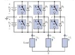
Three phase inverter.JPG

The above attached diagram of a three phase inverter shows a ground between the two sources Vs/2, in comparison to my design these are two capacitors connected in series so that they charges upto Vs/2 respectively.

The diagram below of the three phase low pass filter shows Neutral of the three phase RLC filter to be grounded. Should i be connecting this neutral point to the ground mentioned in the above diagram of inverter. Maybe this is causing the problem?

Three phase low pass filter.JPG
 

If you consider a bit of RF hash flowing down through a filter capacitor, it arrives at the "neutral" point, then where does it go? Up through the other LPF caps into the other FETS? - they may be off? Also the neutral point is neutral wrt the 50 HZ, not to the PWM carrier, because even if the PWM carrier is exactly timed so each pulse is 120 degrees time separated from the others, they will not balance out as they are off equal amplitude (unlike time shifted sine waves). The filter caps should be returned to the PSU 0V, to complete the RF path.
One other possibility springs to mind, if one hi side switch is instantaneously "on", but two lo side switches, the dissipation in the FETs would be different, without any current limiting.
Frank
Frank
 

If you consider a bit of RF hash flowing down through a filter capacitor, it arrives at the "neutral" point, then where does it go? Up through the other LPF caps into the other FETS? - they may be off? Also the neutral point is neutral wrt the 50 HZ, not to the PWM carrier, because even if the PWM carrier is exactly timed so each pulse is 120 degrees time separated from the others, they will not balance out as they are off equal amplitude (unlike time shifted sine waves). The filter caps should be returned to the PSU 0V, to complete the RF path.
A three phase inverter is usually driving the bridge legs with in-phase PWM ("unipolar scheme"). This means that you have a considerable PWM frequent common mode voltage superimposed to the output, e.g. 1/3 of the bus voltage peak-to peak. From an EMC viewpoint it's surely desirable to connect the filter capacitors to DC bus ground (or midvoltage). But inductor and output stage currents will be increased, and particularly a reactive current component added.

If you don't care for switching frequent common mode voltage, you may decide not to ground the filter starpoint.

Regarding the original question "why does one transistor overheat", I fear the threadis lacking necessary detail information. Besides correct gate control waveforms, you should also look for possible DC inbalance. It would show as a DC output current which shouldn't be there.
 

Frank i tested the circuit by connecting the neutral of primary side of the transformer to the neutral of three capacitors and this was connected to the ground of DC which is also connected to the PSU 0V. I had 3A fuses placed in between the Rectifier's DC ouput and Inverters DC bus. These fuses instantly were blown away as i powered on my inverter.

The other possibility of two low side mosfet's being on would also cause the imbalanced current flow when i am directly connecting the load acrosse the inverter.? Although i checked and this isnt the case.

FvM

Thank you for sharing your knowledge over this. :)
As i mentioned above i tried connecting the DC bus ground to the neutral of the capacitors and primary side transformer neutral but it wasnt of much use.
I will be uploading the three gate control pwm waveforms for you to look through and guide me if i made some error while implementing them correctly. Also please let me know whatever you think is needed regarding my design or waveforms at any point, in-order for you to help me find a solution to my problem.
Also can you please guide me how can i check for possible DC inbalance?

- - - Updated - - -

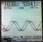
Below is the Ouput across the capacitors of the low pass filter connected in Y configuration. The Voltages are measured phase to phase. The Mosfets are not heating up over 100W load per phase.

IMAG0171.jpg
 

i tested the circuit by connecting the neutral of primary side of the transformer to the neutral of three capacitors
Don't do that, leave the transformer star point floating. Usually a three phase inverter superimposes a 3*f common mode component to increase the available output for a specific bus voltage, it would be shorted by a three-phase transformer with connected star point.

Also can you please guide me how can i check for possible DC inbalance?
Measure the phase-to-phase output voltage, it should be DC-free.
 

Don't do that, leave the transformer star point floating. Usually a three phase inverter superimposes a 3*f common mode component to increase the available output for a specific bus voltage, it would be shorted by a three-phase transformer with connected star point.

so should i leave the star point of the low pass filter capacitors floating as well?

Measure the phase-to-phase output voltage, it should be DC-free

Phase to phase voltages on the primary side of the transformer?
 

so should i leave the star point of the low pass filter capacitors floating as well?
At least for the start. I wonder if you need a filter on the transformer primary side at all? I would think about utilizing the transformer leakage inductance as filter inductance (either additional or without a dedicated inductor).

Phase to phase voltages on the primary side of the transformer?
Yes, presumed you achieve stable operation with transformer. Otherwise connect a resistive test load. The unloaded output should be DC-free as well.
 

Frank i tested the circuit by connecting the neutral of primary side of the transformer to the neutral of three capacitors and this was connected to the ground of DC which is also connected to the PSU 0V. I had 3A fuses placed in between the Rectifier's DC ouput and Inverters DC bus. These fuses instantly were blown away as i powered on my inverter.

The other possibility of two low side mosfet's being on would also cause the imbalanced current flow when i am directly connecting the load acrosse the inverter.? Although i checked and this isnt the case.

FvM

Thank you for sharing your knowledge over this. :)
As i mentioned above i tried connecting the DC bus ground to the neutral of the capacitors and primary side transformer neutral but it wasnt of much use.
I will be uploading the three gate control pwm waveforms for you to look through and guide me if i made some error while implementing them correctly. Also please let me know whatever you think is needed regarding my design or waveforms at any point, in-order for you to help me find a solution to my problem.
Also can you please guide me how can i check for possible DC inbalance?

- - - Updated - - -

Below is the Ouput across the capacitors of the low pass filter connected in Y configuration. The Voltages are measured phase to phase. The Mosfets are not heating up over 100W load per phase.

View attachment 104911


why the frequency is here 54 hz ??

Thankyou for your insights chuckey

The driver IR2109 comprises of an internal dead time to avoid both the high and low side Mosfets be switched on at the same time.

This maybe the cause of leakage inductance. What is your recommendation to solve this problem?

- - - Updated - - -

View attachment 104877

The above attached diagram of a three phase inverter shows a ground between the two sources Vs/2, in comparison to my design these are two capacitors connected in series so that they charges upto Vs/2 respectively.

The diagram below of the three phase low pass filter shows Neutral of the three phase RLC filter to be grounded. Should i be connecting this neutral point to the ground mentioned in the above diagram of inverter. Maybe this is causing the problem?

View attachment 104878


what is the inductor resister and resister value in singlw phase low pas filter ???
 

If you use a scope with a dramatic LPF in series with the probe, so it displays more or less the 50 HZ component and rejects the PWM stuff and accurately inspect the 50 HZ components of each phase to check their amplitude and phase and wave form shape. This may give you a clue as to what the problem is. Generating three phase via software, leaves one to ponder on exactly what is going on, due to unforseen assymetry in the timing of the loops.
Frank
 

Status
Not open for further replies.

Similar threads

Part and Inventory Search

Welcome to EDABoard.com

Sponsor

Back
Top