dkaikas
Newbie level 3
Hello to all,
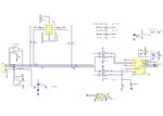
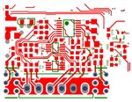
I am designing a system for analog measurement of RTD, Thermocouple & 4-20mA with 2 inputs, using Sigma-Delta ADC converter.
The system is powered from 9->28VDC. This voltage is converter to 5VDC using OKI-78SR switching power supply module. The 5VDC is then fed to BQ24070 LiIon battery charger. This battery charging IC provides 4.4V on the output or the LiIon battery voltage when main power supply is off. Finally, a linear LDO is used to provide 3.3V from 4.4V.
I am facing the following problem and behaviour of the circuit:
- RTD measurement noise is on the order of 0.02 degrees Celsius, which is fine and represents 1 LSB of the ADC. The noise remains the same using battery, external linear 12V power supply (supply A), external switching mode power supply (supply B), and another external switching mode power supply (supply C).
- Thermocouple measurement noise is on the order of 1 LSB using battery, external supply A, supply B, BUT NOT with supply C. When the system is connected to supply C, it measures Thermocouple temperature with an offset of about 3 degrees Celsius when battery charging is off and 30 !! degrees Celsius when battery is charging with about 850mA. Also, there is very high noise except from the offset !!
From the above, I assume that the problem is the noise in power supply which passes to the analog domain of the board. I have noticed that between power supply B and C, there is one more small transformer on the primary side of supply B (the "good" one). Both power supply are "budget price" 12V/1A.
Some facts that might help (using supply C):
- When I connect the system to PC through USB or Serial port (actually connecting PC and system GND together), the problem disappears as long as they remain connected, no matter if the battery is charging
- Using second LDO to produce A3V3 from 4V4 did not solve the problem.
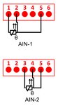
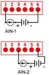
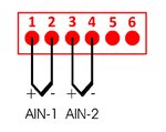
- Removing U14 (DG2731/33 analog switch) solves the problem, so I assume that noise passes from 3V3->A3V3->DG2731/33->AINx+ and AINx-.
The weird thing is that RTD measurement is not affected by the power supply in use but Thermocouple measurement does !!!
The design files:
**broken link removed**
**broken link removed**
**broken link removed**
**broken link removed**
**broken link removed**
Any ideas would be very appriciated because I am struggling to find the problem a long time now. Thank you very much.
Dimitris.
I am designing a system for analog measurement of RTD, Thermocouple & 4-20mA with 2 inputs, using Sigma-Delta ADC converter.
The system is powered from 9->28VDC. This voltage is converter to 5VDC using OKI-78SR switching power supply module. The 5VDC is then fed to BQ24070 LiIon battery charger. This battery charging IC provides 4.4V on the output or the LiIon battery voltage when main power supply is off. Finally, a linear LDO is used to provide 3.3V from 4.4V.
I am facing the following problem and behaviour of the circuit:
- RTD measurement noise is on the order of 0.02 degrees Celsius, which is fine and represents 1 LSB of the ADC. The noise remains the same using battery, external linear 12V power supply (supply A), external switching mode power supply (supply B), and another external switching mode power supply (supply C).
- Thermocouple measurement noise is on the order of 1 LSB using battery, external supply A, supply B, BUT NOT with supply C. When the system is connected to supply C, it measures Thermocouple temperature with an offset of about 3 degrees Celsius when battery charging is off and 30 !! degrees Celsius when battery is charging with about 850mA. Also, there is very high noise except from the offset !!
From the above, I assume that the problem is the noise in power supply which passes to the analog domain of the board. I have noticed that between power supply B and C, there is one more small transformer on the primary side of supply B (the "good" one). Both power supply are "budget price" 12V/1A.
Some facts that might help (using supply C):
- When I connect the system to PC through USB or Serial port (actually connecting PC and system GND together), the problem disappears as long as they remain connected, no matter if the battery is charging
- Using second LDO to produce A3V3 from 4V4 did not solve the problem.
- Removing U14 (DG2731/33 analog switch) solves the problem, so I assume that noise passes from 3V3->A3V3->DG2731/33->AINx+ and AINx-.
The weird thing is that RTD measurement is not affected by the power supply in use but Thermocouple measurement does !!!
The design files:
**broken link removed**
**broken link removed**
**broken link removed**
**broken link removed**
**broken link removed**
Any ideas would be very appriciated because I am struggling to find the problem a long time now. Thank you very much.
Dimitris.