Continue to Site

Welcome to EDAboard.com

Welcome to our site! EDAboard.com is an international Electronics Discussion Forum focused on EDA software, circuits, schematics, books, theory, papers, asic, pld, 8051, DSP, Network, RF, Analog Design, PCB, Service Manuals... and a whole lot more! To participate you need to register. Registration is free. Click here to register now.

Thermal via pad size increased in inner layer while applying copper pour in PADS2005?

Status
Not open for further replies.

kabaleevisu

Advanced Member level 2
Joined
Apr 14, 2010
Messages
616
Helped
85
Reputation
170
Reaction score
81
Trophy points
1,308
Location
Chennai,India
Activity points
4,512
Hi everyone,
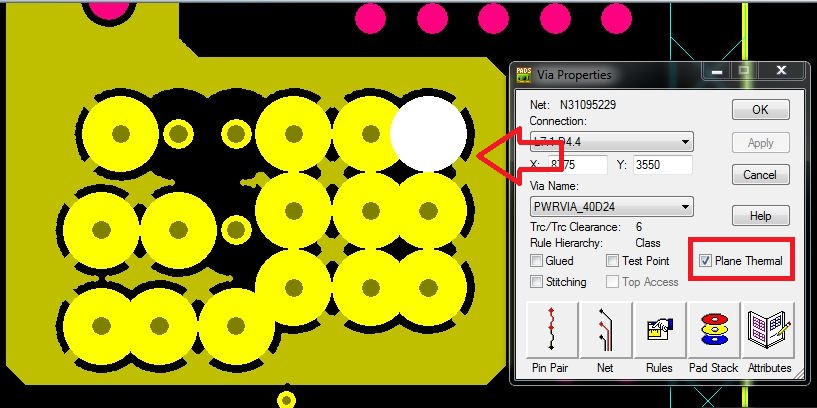
i applied copper pour on inner layer via but inner layer via size is increased ?? it is visiblity problem or is i need to change any setting in option.


You'll want remove the thermal isolation for this vias. Usually isolation doesn't make sense for vias at all.
 

Status
Not open for further replies.

Part and Inventory Search

Welcome to EDABoard.com

Sponsor

Back
Top