Continue to Site

Welcome to EDAboard.com

Welcome to our site! EDAboard.com is an international Electronics Discussion Forum focused on EDA software, circuits, schematics, books, theory, papers, asic, pld, 8051, DSP, Network, RF, Analog Design, PCB, Service Manuals... and a whole lot more! To participate you need to register. Registration is free. Click here to register now.

Thermal Relief and anti pads

Status
Not open for further replies.

LeeHavens

Newbie level 5
Joined
Jun 10, 2013
Messages
9
Helped
0
Reputation
0
Reaction score
0
Trophy points
1
Activity points
136
Hello everyone,

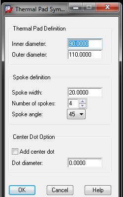
I am struggling with how to create thermal reliefs and anti pads because all I see is the regular pads. Even when I insert the thermal pad in my pads they don't show on my planes, that are turned on in the setup/design parameters. Can someone break down this for me, I am new at all this. So I will need all the small details.

Thank you,
Lee
 

Hi Lee,
for thermal pad you need to create like that file-->New-->select (Flash symbol )from drawing type. and then select Add-->Flash
9416285000_1372388492.png
follow like that
 
Hi Lee,
for thermal pad you need to create like that file-->New-->select (Flash symbol )from drawing type. and then select Add-->Flash
9416285000_1372388492.png
follow like that

Okay this information was very helpful on how to create the thermal relief, but the next problem I run into is I add it to design pad stack and it doesn't appear in my part. I do have it turned on in the setup / design parameters.... So can you help me understand why it is not showing on my pad layers? I am confused on how the pad designer works, can you explain why the regular pad over rides the thermal relief and anti pads?


Thank you,
Lee

P.S. I attached an image to show what I am talking about.
pads.jpg
 

Hang on while I replace the batteries in my crystal ball..... :p

What software are you referring to? It would help people answer your question.
 

Hang on while I replace the batteries in my crystal ball.....
There's a hidden reference to Cadence Allegro, so Allegro users hopefully understand the question. Other edaboard members are apparently meaned to ignore it.

I expect, that the Allegrod manuals can give the answer, too. Definitely not my business.
 

Sorry, Orcad PCB Editor and Pad Designer are the two programs I am using to make the board layout!

- - - Updated - - -

The issue I am having is I used the thermal relief and anti pads in the pad designer to create my pad stacks but when I look at the 3d image the stacks are not correct. I have the thermals turned on in setup/design parameters. If someone can give an example and a walk through of how to do this I would greatly appreciate it. The thermal relief and anti pads are not show on the plans, I am getting just the regular pads.

Thank you,
Lee

Programs used:
Orcad Capture
Orcad Pcb Editor
Pad Designer
 

Hi Lee,

Check whether the shape symbol you have used inside the pad designer for thermal relief and anti-pad are in the same directory of the board file,
and try refreshing. hope it will help you....
 

isn't it available in

tools ---> padstack ---> modify design padstack
then select the required pad
select the "tab layers"
 

isn't it available in

tools ---> padstack ---> modify design padstack
then select the required pad
select the "tab layers"

Yes it is in the "tab layers", and I have them in the thermal relief and anti pads. The problem I am having is all I see is regular pads.... the thermal relief or anti pads don't show up? I don't understand what step I missed or what I am doing wrong. That is why if someone can give me an example or something I can go over and work my way through then I would be able to work through it.
 

Yes it is in the "tab layers", and I have them in the thermal relief and anti pads. The problem I am having is all I see is regular pads.... the thermal relief or anti pads don't show up? I don't understand what step I missed or what I am doing wrong. That is why if someone can give me an example or something I can go over and work my way through then I would be able to work through it.


Thermal Relief and anti pads are only for inner layer that too for negative artwork. We can see this in negative artwork
go to setup---> Cross Section---> click negative artwork for all the planes, then you can see your thermal relief in the pcb editor
 

Status
Not open for further replies.

Part and Inventory Search

Welcome to EDABoard.com

Sponsor

Back
Top