Continue to Site

Welcome to EDAboard.com

Welcome to our site! EDAboard.com is an international Electronics Discussion Forum focused on EDA software, circuits, schematics, books, theory, papers, asic, pld, 8051, DSP, Network, RF, Analog Design, PCB, Service Manuals... and a whole lot more! To participate you need to register. Registration is free. Click here to register now.

the mysterious emitter follower

Status
Not open for further replies.

libyantiger

Member level 5
Joined
Aug 10, 2016
Messages
90
Helped
0
Reputation
0
Reaction score
3
Trophy points
1,288
Activity points
2,269
in this text book "the art of electronics" for horowitz the writer said that the transistor will be shuted down

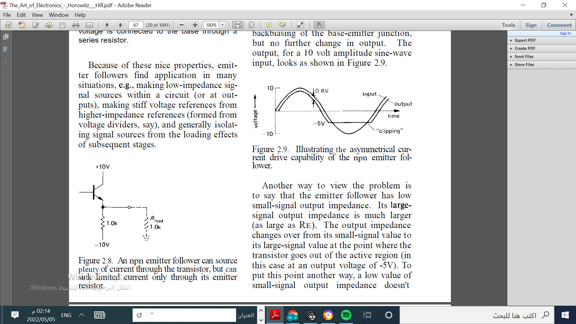
at -5 vdc the output will be cutted like shown


i cant see why the output will be cut

since at -5vdc the emitter base junction will still be forward baised since the -5 vdc is more positive than -10

and thus the transistor will be working normally

any explaination why should the emitter follower stop conduction at -5vdc ?
1651753185951-png.176023
 

Attachments

  • 1651753185951.png
    1651753185951.png
    337.9 KB · Views: 384

Hi,

you missed to care for Rload.

The 1k resistor to -10V and the 1k load resistor form a voltage divider.

Klaus
 
Actually, it's the correct answer.
so the correct answer is no asnwer???

--- Updated ---


Hi,

you missed to care for Rload.

The 1k resistor to -10V and the 1k load resistor form a voltage divider.

Klaus

can you explain "intuitvly" why should the transistor shuted at -5 you indicated the load is somewhat severe that is why the transistor is shuted

lets assume that we are "loading the transistor too much " what is actually happens that pushs the transistor out of conduction
 

As the base approaches - 5 the transistor presents less load on the 1K 1K
V divider, so its V approaches -5 of the divider when it is unloaded by transistor.

So with base at -5 and emitter (R divider junction) at -5, the transistor is off
and the V stays at the divider - 5 = "cutted".

Notice the Vcut is when Vbase + Vbe = -5. Or Vbase =~ -4.5

1651797041303.png


1651797210158.png


Regards, Dana.
 
Last edited:

still not get good answer why the out is cutted
Did you do the calculation I suggested in post #3?
If so it should be obvious why the output is clamped at that voltage.

Remember that the emitter follower can only provide current in one direction.
 

Solution
As the base approaches - 5 the transistor presents less load on the 1K 1K
V divider, so its V approaches -5 of the divider when it is unloaded by transistor.

So with base at -5 and emitter (R divider junction) at -5, the transistor is off
and the V stays at the divider - 5 = "cutted".

Notice the Vcut is when Vbase + Vbe = -5. Or Vbase =~ -4.5

View attachment 176030

View attachment 176031

Regards, Dana.
first thanks dana for your effort you did a fantastic job with the simulations

second if am not mistaken it is like the following


since the emitter voltage is held at -5 as resualt of voltage divider once the vbe reachs to -5vdc there is net 0 vdc result across

the diode junction base-emitter and thus the transistor will shut down as ressult


i have not noticed that it was a divider a simple voltage divider and thus all my "see guess" analysis gone in vain


thanks dana corrrect me if i am wrong please
 

Your conclusion partially correct.

The divider does not "hold" / determine the voltage until the transistor is off.
Up to that point it affects but is only partial reason for divider node V. Due
to transistor, when conducting, dumps current into the node. But once the
Vbe collapses and transistor turns off then divider sets the node V.

Regards, Dana.
continuing with the emitter follower complications why do you think vbe is never 0.6 it is always 1.5 vdc or more in the shown circuit


the circuit works fine and as expected


this circuit is a study of how follower used as current source

since the base circuit consist of 4.6vdc and vbe which is 0.6 the transistor should have ve of 4vdc all the time

since vbe 4.6 minus vbe which is 0.6 gives us ve of 4vdc ....ve over re which is 4 ohm is 1 amp


that 1 amp should alwyas pass trough the load resistor rc which should all the time get 1 amp

except the moment at which the value of the reistor will cause voltage across it that exceed vcc at that point kershov rule prevail

and the current source will no longer works fine

made 2 cases one at which 4 ohm was the rc load reisstor the circuit work as expected "thogh 1.6 is never expected" and 1 amp pass through load reisistor which is demonstration of current source being valid


first case load resistor was 30 ohm if 1 amp passed now the entire vcc will not be enough to satisfy that so kershof rule prevail
and the ic will be much lesser than ie and the current source will no longer be valid

all is as expected but to me why the vbe is not 0.6 ?

1652473780445.png


1652473598012.png
 

You are driving base hard to get the 800 mA in the collector, and this parts
base spreading R significant. If the below curve was extended to see higher
currents you would see the high Vbe....

1652483873610.png


Regards, Dana.
 

You are driving base hard to get the 800 mA in the collector, and this parts
base spreading R significant. If the below curve was extended to see higher
currents you would see the high Vbe....

View attachment 176180


Regards, Dana.
--- Updated ---

but according to what teachers thought me the vbe always take 0.6 and toss what ever voltage left over the other parts of the circuits like
resistors we always think of diodes and vbe junctions this way ?? so i have not forced any thing over 0.6 or over drived the transistor ?
what say you?
 

Either your teachers are wrong, or you misunderstood. Vbe is nominally .6 to .7 volts, but as the curves plainly show, it increases with collector current. It is not "always" 0.6V, that's just a rough estimate.
 

Either your teachers are wrong, or you misunderstood. Vbe is nominally .6 to .7 volts, but as the curves plainly show, it increases with collector current. It is not "always" 0.6V, that's just a rough estimate.
that is a completely new piece of info thanks man
 

Hi,

there are so called normal operating conditions.

A car battery is named 12V. But under normal operating conditions it is 11V ... 14.4V. For sure you may "mistreat" it and "over discharge" it to less than 11V (or more than 14.4V). You may do this, but it will sooner or later kill the battery.

A LED may be specified for 2.2V. You may mistreat it and force 3V into it. It may explode then.

A Vbe may be 0.6V ... you may force it to be 1V .... and you will kill it.
That's what you do.
--> treat it normally and it will behave normally.

Klaus
 

Emitter Base junction looks very similar to a diode response.

Classic diode -

1652521964562.png


LED Diode -

1652521997723.png


Its not unusual to exceed .6V when driving a transistor into saturation (using it as a switch), 2N2222 example -

1652524250648.png


Here is a power transistor 2N3055 -

1652524938746.png


Regards, Dana.
 
Last edited:
Emitter Base junction looks very similar to a diode response.

Classic diode -

View attachment 176181


LED Diode -

View attachment 176182


Its not unusual to exceed .6V when driving a transistor into saturation (using it as a switch), 2N2222 example -

View attachment 176185

Here is a power transistor 2N3055 -

View attachment 176186


Regards, Dana.
BUT in almost all text book it is always assumed that diode only drops its usuall forward diode drop voltage and "toss" the left voltage on the resistor ? so it is not like that even for the diode and the diode is supossed to accept diffrenet voltage across it as currnt increase or decrease through it
 

Hi,

every device has it´s limits.

A bungee rope: when you overload it, it becomes longer and longer, then it bursts.
An incandescent 12V, when driven with overly high voltage becomes brighter and brighter until it burns.
A tyre will also burst when you put too much air pressure in.
A cake will burn when the oven is too hot.

Some people accept limits.
I mean: is it necessary to desribe in "textbooks" what happens when you overload and mistreat things?

I´d say it´s sufficient that "datasheets" specify the limits. And textbooks focus on the behaviour at normal operating conditions.

Klaus
 
Last edited:

BUT in almost all text book it is always assumed that diode only drops its usuall forward diode drop voltage and "toss" the left voltage on the resistor ? so it is not like that even for the diode and the diode is supposed to accept different voltage across it as current increase or decrease through it

The common assumption that Vbe on is relatively fixed fits the fact many transistors
operated as amplifiers, so at those bias levels the .6V, .7V make sense. But its clear when
one starts talking about power, such as in PA's, large load switching, etc.. that larger Vbe
occurs. Not a disturbing fact, just simply one that occurs because of junction behavior.

Interesting but alarming, is very few datasheets spec base current absolute maximums, at
least the few I have used and worked with. Seems like an omission to me.

Regards, Dana.
 
Last edited:

Status
Not open for further replies.

Part and Inventory Search

Welcome to EDABoard.com

Sponsor

Back
Top