Continue to Site

Welcome to EDAboard.com

Welcome to our site! EDAboard.com is an international Electronics Discussion Forum focused on EDA software, circuits, schematics, books, theory, papers, asic, pld, 8051, DSP, Network, RF, Analog Design, PCB, Service Manuals... and a whole lot more! To participate you need to register. Registration is free. Click here to register now.

The efficiency of rectifier is too low when using ADS layout.

Status
Not open for further replies.

True koke

Newbie level 6
Joined
Apr 15, 2022
Messages
13
Helped
0
Reputation
0
Reaction score
2
Trophy points
1
Activity points
199
I'm using ADS to check the efficiency of voltage doubler, but there are something problems.
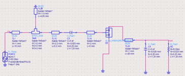
I designed the rectifier like below image and i did simulation in EM simulation that ADS support.
In the 2D circuit, the efficiency of rectifier is about 60%.
However when I did simulation using Layout with EM simulation, the rectifier's efficiency is too low.(about 13~14%)
I set the layout only microstrip lines without any components like diode, capacitor, resistor.
I made the symbol to export to in my circuit and then I located the components using wires.

OC.PNG

Lay.PNG

symbol.PNG

Please answer what are the problems.
Thanks.
 

You schematic model uses MLIN, but your layout in Momentum has additional side grounds with ~1mm gaps. If substrate is thick (e.g. 1.5mm FR4) these side grounds at 1mm distance have a visible effect on line impedance.

In addition: Are you sure that line widths in layout match values from schematic? For example the MLSC TL22 is wider than input line according to schematic value, but in layout look-alike it looks narrower.

I think you just have too much difference layout vs. schematic models. In addition, double check that your shorted line has a via at the end in Momentum. Momentum newbies often forget to map the via layer in their Momentum stackup. Placing ground symbols in layout does nothing for Momentum, you need to have physical vias there.
 
Last edited:

You schematic model uses MLIN, but your layout in Momentum has additional side grounds with ~1mm gaps. If substrate is thick (e.g. 1.5mm FR4) these side grounds at 1mm distance have a visible effect on line impedance.

In addition: Are you sure that line widths in layout match values from schematic? For example the MLSC TL22 is wider than input line according to schematic value, but in layout look-alike it looks narrower.

I think you just have too much difference layout vs. schematic models. In addition, double check that your shorted line has a via at the end in Momentum. Momentum newbies often forget to map the via layer in their Momentum stackup. Placing ground symbols in layout does nothing for Momentum, you need to have physical vias there.
Thanks for your reply.

I modified the layout to match 2.45GHz.
I understand how to connect the Via in lay.
But even though it is well matched, the rectifier's efficiency is too low.

Is there anything wrong with the wire connection after importing the EM model into the circuit? Or is there something wrong with the layout design itself?
(For your information, I modified the layout for matching, so you don't need to advise the thickness or length of ML)

Please refer to the below image I have designed.
2Dc.PNG

EMsymbol.PNG

Layout.PNG
 

Attachments

  • 2Dc.PNG
    2Dc.PNG
    29.4 KB · Views: 186

There are many mistakes and many differences between layout and schematic.

For MTEE, the width parameters are the widths of the lines connected there. You have other values. That is just one example where your schematic model isn't accurate.

Much worse here is your shunt branch: in schematic you have w=1.9mm and l=4.05mm but in layout that line looks really different. There are more of these inconsistencies in other elements, e.g. width of TL10 and TL19.

And there is an extra ground via pad section, connected by ideal wire in schematic ... why did you do this? That layout path adds path length (inductance) that is not included in your schematic model. It is expected that these large differences in layout (drawn vs. model) show in results.

~~

Regarding via, please show your Momentum substrate, to make sure the via layer ("hole") is properly mapped there.

~~

You switched layout from GCPW to microstrip. The advantage is that microstrip layout can be modelled using schematic models, which don't exist in ADS for CPWG. But your initial layout looked much better, from an RF routing perspective. It just can't be modelled using simple schematic elements so easily.
 
Last edited:

There are many mistakes and many differences between layout and schematic.

For MTEE, the width parameters are the widths of the lines connected there. You have other values. That is just one example where your schematic model isn't accurate.

Much worse here is your shunt branch: in schematic you have w=1.9mm and l=4.05mm but in layout that line looks really different. There are more of these inconsistencies in other elements, e.g. width of TL10 and TL19.

And there is an extra ground via pad section, connected by ideal wire in schematic ... why did you do this? That layout path adds path length (inductance) that is not included in your schematic model. It is expected that these large differences in layout (drawn vs. model) show in results.

~~

Regarding via, please show your Momentum substrate, to make sure the via layer ("hole") is properly mapped there.

~~

You switched layout from GCPW to microstrip. The advantage is that microstrip layout can be modelled using schematic models, which don't exist in ADS for CPWG. But your initial layout looked much better, from an RF routing perspective. It just can't be modelled using simple schematic elements so easily.

Thanks for your reply.

As I said above, the Layout was modified for matching 2.45GHz.

I designed layout, made the symbol, did the simulation only Microstirp lines without any components like Diode, Capacitors, Resistor.

And then I made the wires to connect the C,R,Diode to ML after importing the symbol I made into circuit.

Could you please check the attached recorded video regarding how to set the simulation?
This is the very important problem what shoul i have to do.
Thanks in advance.
 

I understand that you modified the layout, but you also showed a schematic model representation of the layout which disagreed with your drawn layout. My understanding was that both views are up-to-date for 2.45 GHz and your issue was the difference in results.

Modelling of your layout in the video looks ok, EM stackup looks ok, and the MLSC has the required sheet via at the end. So your Momentum result looks trustworth.
Thanks for your reply.

I extend the result of frequencies upto 10GHz, there are another resonance points.
So i think that's why the efficiency was too low at 2.45Ghz.

But I have a one more question about Layout tool in ADS.
I want to place the Port1 at the start of substrate to connect HW cable when I'll make the PCB board like below image.
board layout.PNG


When I see the 3D EM preview in ADS Layout, it is not.
And I just cut the plane in 3D EM preview, is it right way? or is there other way to place the port1 at the start?

Please check the below image.
Cutplane.PNG
 

Higher resonances are expected because you use transmission line matching, and you just rotate multiple times in Smith chart.

Not sure if I understand your question about port 1. If you open the ports editor in layout, you can map layout pins to EM ports. From what I can see in your screenshot, you want to have Pin1 as Port 1 Plus and Pin10 as Port 1 Minus. Such explicit port ground is set in port editor, see example below. Use drag & drop in the ports editor to move Pin10 to the minus terminal. By default, the minus terminal is at global ground = substrate backside. However, there is little effect of that change in your case, because the path from Pin10 ground to substrate backside is short.

I can't comment on your circuit structure, but 2.4 GHz rectifier student projects are discussed here on edaboard very often.

Just one detail that I noticed: your MLSC is a line with SHORTED end, the picture that you show has an OPEN ended stub from what I can see.


diffpins.png

--- Updated ---

Regarding ports again: it is also possible to connect your schematic port between two EM model ports, as you did. For the EM model data you then have two ports to global ground (substrate backside) but the schematic port connection then does what you wanted. There is no problem with your port connection.
 
Last edited:

Higher resonances are expected because you use transmission line matching, and you just rotate multiple times in Smith chart.

Not sure if I understand your question about port 1. If you open the ports editor in layout, you can map layout pins to EM ports. From what I can see in your screenshot, you want to have Pin1 as Port 1 Plus and Pin10 as Port 1 Minus. Such explicit port ground is set in port editor, see example below. Use drag & drop in the ports editor to move Pin10 to the minus terminal. By default, the minus terminal is at global ground = substrate backside. However, there is little effect of that change in your case, because the path from Pin10 ground to substrate backside is short.

I can't comment on your circuit structure, but 2.4 GHz rectifier student projects are discussed here on edaboard very often.

Just one detail that I noticed: your MLSC is a line with SHORTED end, the picture that you show has an OPEN ended stub from what I can see.


View attachment 175584
--- Updated ---

Regarding ports again: it is also possible to connect your schematic port between two EM model ports, as you did. For the EM model data you then have two ports to global ground (substrate backside) but the schematic port connection then does what you wanted. There is no problem with your port connection.
Thanks for your reply.

I mean that port1 be located at the start of PCB board like attached image yesterday.
If I make the PCB board to measure, the Port1 must be located at the end because the antenna will be connected to Port1.
But when I open the 3D EM Preview, the Port1 is not at the end of substrate.
More intuitively, when I open the 3D EM Preview the result is like below.
3ddddd.PNG


Port1 must be located at the end of the substrate like the picture below.
Because I have to connect the antenna at the port1.!

hw.PNG
 

Attachments

  • board layout.PNG
    board layout.PNG
    241.1 KB · Views: 107

Don't worry about the purple PCB outline that you see. Momentum simulates with an infinite substrate size, there is no PCB boundary in Momentum. No need for change!
 

Status
Not open for further replies.

Part and Inventory Search

Welcome to EDABoard.com

Sponsor

Back
Top