Continue to Site

Welcome to EDAboard.com

Welcome to our site! EDAboard.com is an international Electronics Discussion Forum focused on EDA software, circuits, schematics, books, theory, papers, asic, pld, 8051, DSP, Network, RF, Analog Design, PCB, Service Manuals... and a whole lot more! To participate you need to register. Registration is free. Click here to register now.

text and text overlapping clearance error in pads router

Status
Not open for further replies.

robismyname

Full Member level 6
Joined
Jan 17, 2008
Messages
390
Helped
11
Reputation
22
Reaction score
9
Trophy points
1,298
Location
Central Florida
Activity points
4,603


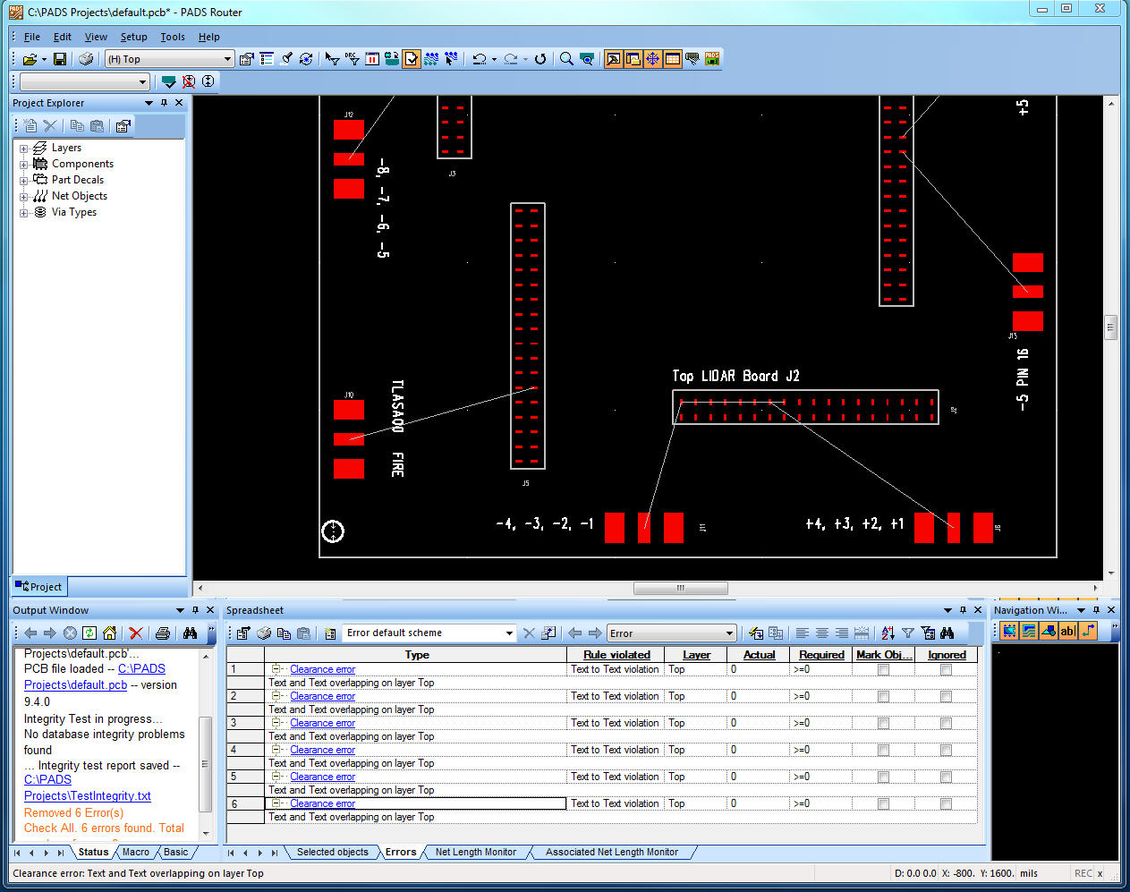
Cant resolve the attached trivial issue in pads router. Some sort of clearance error related to my text that pads router will not point me to directly so i dont know where the problem is.

Any pointer on how to resolve this issue?

Also what is that white circle with the two arrows pointing inward in the bottom left of my screen? this came up after I executed "verify design"
 

i think text has you mention in top layer it is should be silkscreen top check the text "layer" ??
 

Status
Not open for further replies.

Part and Inventory Search

Welcome to EDABoard.com

Sponsor

Back
Top