Continue to Site

Welcome to EDAboard.com

Welcome to our site! EDAboard.com is an international Electronics Discussion Forum focused on EDA software, circuits, schematics, books, theory, papers, asic, pld, 8051, DSP, Network, RF, Analog Design, PCB, Service Manuals... and a whole lot more! To participate you need to register. Registration is free. Click here to register now.

Tested SMPS circuit is not working with new PCB design

Status
Not open for further replies.

udhay_cit

Full Member level 6
Joined
May 16, 2008
Messages
346
Helped
37
Reputation
74
Reaction score
37
Trophy points
1,318
Activity points
3,895
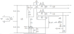
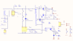
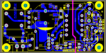
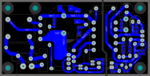
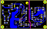
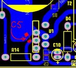
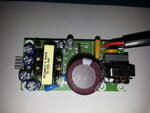
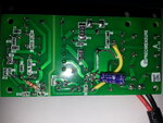
My SMPS is designed with the help of PIExpert & Its rated for +5V/1A, +24V/500mA. The design is tested with 1st version of PCB design (Bigger one) & its working fine. The same PCB is redesigned for size optimization. Now the PCB is not working. I have assembled 2 PCB of new design & both not working. While testing the output with DSO, the controller trying to oscillate & immediately turned off. So some frequent spikes of voltages are appear at the DC output terminals. Unfortunately I can't use the working PCB due to the size consideration.

Please advise me to solve the problem. I can redesign the circuit with 2 layer PCB also but I want to know which side (Primary of secondary) & what correction I should be do for my next design. Any commands will be helpful to me...

Thanks & Regards
Udhay
 

Attachments

  • PiExpert.PNG
    PiExpert.PNG
    25.3 KB · Views: 117
  • Capture.PNG
    Capture.PNG
    59.5 KB · Views: 128
  • PCB.PNG
    PCB.PNG
    154.8 KB · Views: 123
  • Cu only.PNG
    Cu only.PNG
    138.5 KB · Views: 113
  • working.PNG
    working.PNG
    166.3 KB · Views: 128

The polarity of the transformer winding is wrong in the second schematic, hopefully that's not actually how the real circuit is built, right?

Other than that the schematics are practically identical, so my first guess is a flaw in the assembly, second would be a flaw in the layout. What does your DSO show at the D, V, and C pins of the controller?
 

Try to move C5 as drawn
 

Attachments

  • try.JPG
    try.JPG
    19.9 KB · Views: 100

The polarity of the transformer winding is wrong in the second schematic, hopefully that's not actually how the real circuit is built, right?

Other than that the schematics are practically identical, so my first guess is a flaw in the assembly, second would be a flaw in the layout. What does your DSO show at the D, V, and C pins of the controller?
Sorry for the schematic error. This is the already available schematic symbol which is not match with my transformer. I corrected that in PCB design & the first design is working fine & tested for upto +/- 3.5KV power line surge. I will post the voltage waveform today. I know that the problem is from PCB design, but before I start my redesign I want to know what correction I should be made. Because I dont want to do the same mistake again.


Try to move C5 as drawn
I added an additional capacitor of 0.1µF as you mentioned. Not working :thumbsdown:. I decide to add an additional electrolytic capacitor very near by the pin. Still not working:bang:.

Regards
Udhay
 

Attachments

  • 20150515_111510.jpg
    20150515_111510.jpg
    598.1 KB · Views: 106
  • 20150515_111532.jpg
    20150515_111532.jpg
    936.8 KB · Views: 126

electrolytic cap is not need. C5 must be ceramic.
cap C5 and circuit R11-C14 have to be connected directly between C and S pins of the TOPswitch. in this part your first pcb is better.
can you show oscillograms at output 5v and C, D pins?
 

Status
Not open for further replies.

Similar threads

Part and Inventory Search

Welcome to EDABoard.com

Sponsor

Back
Top