bellona
Junior Member level 2
Hi, everyone, I have taped out a readout chip ( 3.3V 0.35um 2P4M process )for my MEMS sensor and part of it is not functioning as I intended, so I’m looking forward to any suggestions that you might kindly give.
In this chip I have a fully differential transimpedance amplifier for monitoring the displacement current generated by MEMS resonators, and I found there is something wrong with this amplifier's CMFB circuitry. The schematic of this amplifier and its test setup is in the attachment. (Note that in the test setup, CF1,CF2 ,SW1 and SW2 are intended for other high-gain applications and is included in the OPAMP cell, since the impedance of CF1 and CF2 are much higher than RF1 and RF2 at the frequency of interest (6KHz) , I didn't bother to remove it from layout.)
The opamp is adapted from Banu's design (M. Banu, et al., "Fully differential operational amplifiers with accurate output balancing," Solid-State Circuits, IEEE Journal of, vol. 23, pp. 1410-1414, 1988.),The CMFB circuitry is formed by MN12, MN9, MN10, MP10, MP11,MP3 and MP4. I made the differential pair of MN9 and MN10 unsymmetrical in case the input pair MP0 and MP1 is shut down and the current of MP3 and MP4 are not sufficient to restore the output common mode voltage.
I thought at first the CMFB circuit would work fine at any input range that keeps MN12, MN10 and MP11 in saturation, which is about 1.1V at the low end. Post layout simulation also verified that when VCM=1.2V the circuit would function alright.
But when I Powered on the test setup with a VCM about 1.4V, the common mode output of the amplifier is only about 500mV.
When VCM is increased to about to 1.6V, one of the output (OUTN) starts kicking upwards, but the output is not stable and is still far from VCM.
Since both output is quite low, at first I suspect that maybe the startup circuit isn't working and the OPAMP is not biased right. I made a probe pad with FIB at the drain of MN16 and inserted a 1Mohm resistor between that node and VDD, but the result is about the same.
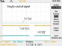
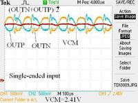
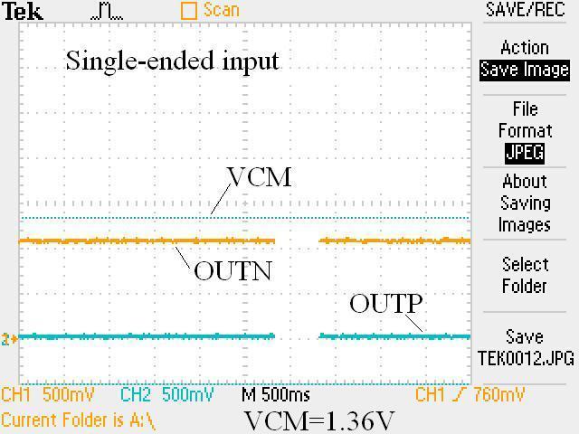
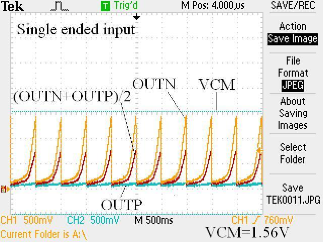
Later on I find out that I have to apply a high VCM (>3V) to kick start this circuit. when VCM is above 3V I got both output railed near VDD. once the output is high, I can lower VCM to a more operable region. When the input is single-ended (a 6KHz sinusoidal signal), I find the optimum VCM input is around 1.88V.
The waveform for different VCM is attached below.

As can be seem from above figure, the output is very asymmetrical, the output is only symmetrical around VCM of 1.88V. when VCM is lowered to 1.6V both output would suddenly drop and the circuit resumes the state I mentioned earlier.
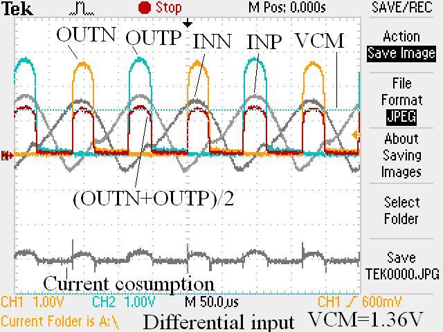
I also did a experiment with fully differential input, I find out that when the output is low I can apply a very large differential signal ( 6KHz sinusodial )at the input and the corresponding output would be high for a brief period of time.
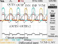
Note that CMFB is also functioning during that period of time, since the top portion of the output common-mode lines up with VCM. I also measured the dynamic current consumption of my chip, which shows that during that time the current dissipation is decreased by about 200uA (bump means decreased current since I used a transimpedance amplifier to monitor the current flowing out of chip's GND).
My questions are:
1. Since the biasing of my circuit is right, the only plausible answer for the low output is that the gate of MN5 and MN7 is way too high, which suggests the CMFB might be dumping too much current through MP3 and MP4 (hence the increased current cosumption when output is low). But why should there be any current flowing when the output common mode is so low?
2. When I have kicked start this circuit with high input VCM, it should work as a single-ended to differential converter When it's feed with single-ended input. But the output is very asymmetrical, as can be seem from above figure, the output is only symmetrical around VCM of 1.88V. So what's causing all these asymmetries?
3. My CMFB circuit seems to be causing all these problems, so what's wrong with this CMFB circuit? Is it because it's unsymmetrical or I should have two CMFB circuit for this two stage opamp?
Also attached is the simulated DC operating points of the MOSFETS (At VCM=1.2V). There are some flaws in the design, such as resistances of R1 and R2 are a little small which decrease the headroom of cascode devices like MP17 and MN18, and it's more approporiate to set the W/L of MN0 and MN1 to 30/1, But I don't think these would cause much trouble.
Any suggestion is highly appreciated, thanks in advance!
In this chip I have a fully differential transimpedance amplifier for monitoring the displacement current generated by MEMS resonators, and I found there is something wrong with this amplifier's CMFB circuitry. The schematic of this amplifier and its test setup is in the attachment. (Note that in the test setup, CF1,CF2 ,SW1 and SW2 are intended for other high-gain applications and is included in the OPAMP cell, since the impedance of CF1 and CF2 are much higher than RF1 and RF2 at the frequency of interest (6KHz) , I didn't bother to remove it from layout.)
The opamp is adapted from Banu's design (M. Banu, et al., "Fully differential operational amplifiers with accurate output balancing," Solid-State Circuits, IEEE Journal of, vol. 23, pp. 1410-1414, 1988.),The CMFB circuitry is formed by MN12, MN9, MN10, MP10, MP11,MP3 and MP4. I made the differential pair of MN9 and MN10 unsymmetrical in case the input pair MP0 and MP1 is shut down and the current of MP3 and MP4 are not sufficient to restore the output common mode voltage.
I thought at first the CMFB circuit would work fine at any input range that keeps MN12, MN10 and MP11 in saturation, which is about 1.1V at the low end. Post layout simulation also verified that when VCM=1.2V the circuit would function alright.
But when I Powered on the test setup with a VCM about 1.4V, the common mode output of the amplifier is only about 500mV.
When VCM is increased to about to 1.6V, one of the output (OUTN) starts kicking upwards, but the output is not stable and is still far from VCM.
Since both output is quite low, at first I suspect that maybe the startup circuit isn't working and the OPAMP is not biased right. I made a probe pad with FIB at the drain of MN16 and inserted a 1Mohm resistor between that node and VDD, but the result is about the same.
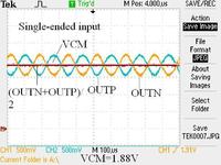
Later on I find out that I have to apply a high VCM (>3V) to kick start this circuit. when VCM is above 3V I got both output railed near VDD. once the output is high, I can lower VCM to a more operable region. When the input is single-ended (a 6KHz sinusoidal signal), I find the optimum VCM input is around 1.88V.
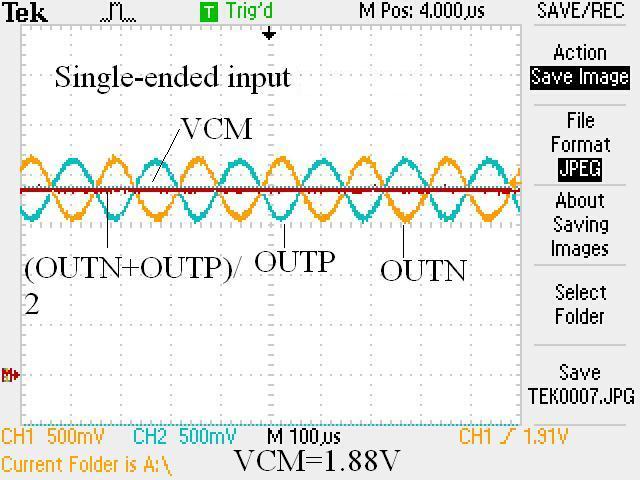
The waveform for different VCM is attached below.
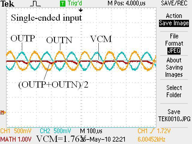
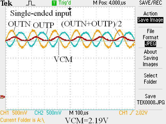
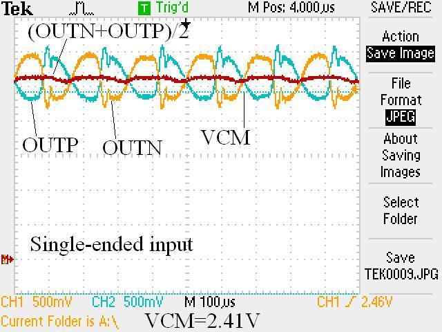
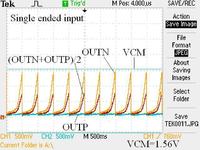
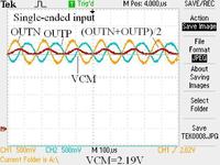
As can be seem from above figure, the output is very asymmetrical, the output is only symmetrical around VCM of 1.88V. when VCM is lowered to 1.6V both output would suddenly drop and the circuit resumes the state I mentioned earlier.
I also did a experiment with fully differential input, I find out that when the output is low I can apply a very large differential signal ( 6KHz sinusodial )at the input and the corresponding output would be high for a brief period of time.
Note that CMFB is also functioning during that period of time, since the top portion of the output common-mode lines up with VCM. I also measured the dynamic current consumption of my chip, which shows that during that time the current dissipation is decreased by about 200uA (bump means decreased current since I used a transimpedance amplifier to monitor the current flowing out of chip's GND).
My questions are:
1. Since the biasing of my circuit is right, the only plausible answer for the low output is that the gate of MN5 and MN7 is way too high, which suggests the CMFB might be dumping too much current through MP3 and MP4 (hence the increased current cosumption when output is low). But why should there be any current flowing when the output common mode is so low?
2. When I have kicked start this circuit with high input VCM, it should work as a single-ended to differential converter When it's feed with single-ended input. But the output is very asymmetrical, as can be seem from above figure, the output is only symmetrical around VCM of 1.88V. So what's causing all these asymmetries?
3. My CMFB circuit seems to be causing all these problems, so what's wrong with this CMFB circuit? Is it because it's unsymmetrical or I should have two CMFB circuit for this two stage opamp?
Also attached is the simulated DC operating points of the MOSFETS (At VCM=1.2V). There are some flaws in the design, such as resistances of R1 and R2 are a little small which decrease the headroom of cascode devices like MP17 and MN18, and it's more approporiate to set the W/L of MN0 and MN1 to 30/1, But I don't think these would cause much trouble.
Any suggestion is highly appreciated, thanks in advance!