Continue to Site

Welcome to EDAboard.com

Welcome to our site! EDAboard.com is an international Electronics Discussion Forum focused on EDA software, circuits, schematics, books, theory, papers, asic, pld, 8051, DSP, Network, RF, Analog Design, PCB, Service Manuals... and a whole lot more! To participate you need to register. Registration is free. Click here to register now.

Synthesizing 3NAND + 1INV : GAL's with PALASM

Status
Not open for further replies.

monahanz

Junior Member level 1
Joined
Nov 11, 2013
Messages
19
Helped
0
Reputation
0
Reaction score
0
Trophy points
1,281
Location
San Ramon CA
Activity points
1,490
Could somebody help me on this what I'm sure is a trivial PALASM question.
Starting with this schematic:-

5196720800_1395633991.jpg


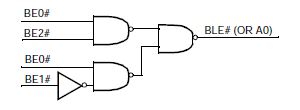
There are 3 NAND gates and one Inverter (input BE1*)
I want to burn a GAL using the four inputs to get the A0 output with PALASM

Since PALSAM does not accept brackets in its EQUATIONS how do I combine the two inputs to the right hand side NAND.

I know I could make two intermediate pins and do this:-

X = \BE0 * \BE2
Y = \BE0 * BE1
/A0 = X * Y

But this uses up two (useless) pins. I considered
A0 = \BE0 * \BE2
+ \BE0 * BE1

But that does not give the correct state
 
Last edited by a moderator:

The last equation looks correct. It should implement the original drawing. I'm not sure what is telling you that it gives the incorrect state.
 

Appreciate the response thanks ads-ee. I may have a GAL programmer problem. I am going to actually breadboard the NAND chips along with the GAL and compare. But good to know I understand the logic.

While I have you, could I get help on one further PALASM question...?
I want to build an S100 bus 80486 CPU board that allows 8 and 16 bit data busses. The Intel hardware manual is great in giving details how to do this. I am attaching the relevant pages. They suggest a PAL to handle the four 8 bit data sections (shifting) the higher 8 bits down to the lower 8 bits data lines etc. They include the following PALASM equations.

CHIP MYPAL1 PALCE22V10 ; Device not selected
;---------------------------------- PIN Declarations ---------------
PIN 1 ADS ;1 COMBINATORIAL ;
PIN 2 BE0 ;2 COMBINATORIAL ;
PIN 3 BE1 ;3 COMBINATORIAL ;
PIN 4 BE2 ;4 COMBINATORIAL ;
PIN 5 BE3 ;5 COMBINATORIAL ;
PIN 6 BS8 ;6 COMBINATORIAL ;
PIN 7 BS16 ;7 COMBINATORIAL ;

Pin 14 BEN8H ;14 COMBINATORIAL ;
Pin 15 BEN8UL ;15 COMBINATORIAL ;
Pin 16 BEN8UH ;16 COMBINATORIAL ;
Pin 17 BEN16 ;17 COMBINATORIAL ;

;----------------------------------- Boolean Equation Segment ------
EQUATIONS

/BEN8H = ADS * BE1 * /BE0 * BS8
+ /ADS * BEN8H

/BEN8UL = ADS * BE2 * /BE1 * /BE0 * BS8
+ /ADS * BEN8UL

/BEN8UH = ADS * BE3 * /BE2 * /BE1 * /BE0 * BS8
+ /ADS * BEN8UH

/BEN16 = ADS * BE2 * /BE1 * /BE0 * BS16 * /BS8
+ BE3 * /BE1 * /BE0 * /BS16 * /BS8
+ /ADS * BEN16

I understand the first line in each equation completely. But what is the second line for. What does the +/ADS * BENxx actually do. I realize pin one is/can be, a clock input on this chip, but the outputs are not register outputs.
 

Attachments

  • Pages 253-265 from 80486 Hardware_Reference_Manual.pdf
    870 KB · Views: 48

The equations on 7-8 shows BEN8H = ADS *BE1*/BE0*BS8 + /ADS*BEN8H

The document says the ADS# is an address strobe, so it looks like if it's active the BEN8H state is held based on the above equation.
 

Well read the document you posted, all I did was quickly scan through it.

The /ADS*BEN8H latches the BEN8H produced by ADS*BE1*/BE0*BS8, beyond that I don't know why they did that. I didn't "read" the document...that's your job.
 

The equations aren't right, you have implemented an inversion (also for the latch feedback) by making the output active low.
Code:
/BEN8H = ADS * BE1 * /BE0 * BS8
+ /ADS * BEN8H

/BEN8UL = ADS * BE2 * /BE1 * /BE0 * BS8
+ /ADS * BEN8UL

/BEN8UH = ADS * BE3 * /BE2 * /BE1 * /BE0 * BS8
+ /ADS * BEN8UH
 

Very good point FvM, thanks! I was trying to take into account that OE (output enable) on any 74Lxxx buffer I can find uses an active low to OE the chip. The hardware manual does not define the actual chip recommended other than they are bidirectional. This would suggest a 74LS245, but again the OE is low.

What really has me confused is that the actual 486 interface buffers (0, 1, 2, 3) use BE0*-3* which are active low. The diagram (Fig7-4) kind of implies the same for buffers 4, 3 & 6. Clearly one can invert BEN8H, BEN8UL and BEN8UH with 74LS04's outside the GAL. But this makes no sense, why not do it within the GAL. Why then do they suggest these equations.

BTW, is there an 8 bit bidirectional buffer that utilizes an active high OE? That would explain it.

Ads-ee I am fully aware of what my job is. The problem being the Intel documentation does not explain the PALASM equations, it just states them. I’m sure no doubt they are clear to seasoned programmers, my goal – not being one of these, was to seek help on this forum from somebody who would be generous enough with their time and knowledge to explain the issue or at least point me in the right direction.
 

You can output inverted enable signals, but then I think the latch feedback term must be inverted, too. It might work to define the signal itself as inverted. It's about twenty years that I've worked with PALASM...
 

As FvM suggest you should use equations like the following (using my 20 year old knowledge)
Code:
/BEN8UH = ADS * BE3 * /BE2 * /BE1 * /BE0 * BS8
+ /ADS * /BEN8UH
I'm not entirely sure the inverted BEN8UH with the /ADS will work or not. If it doesn't you'll have to invert the RHS equation (with the inverted BEN8UH) and convert it back to a sum of products (though it's been so long, since I worked with PALASM I can't be sure about anything).

regards
 

For anybody else that may at some point later be interested interfacing an 80386 with GAL’s I now think I have figured out what’s going on – thanks for pointers guys.

Intel is using active negative logic for the PAL/GAL inputs. It becomes clear if you use positive input logic for the input pins. So we end up with:-

/BEN8H = ADS * /BE1 * BE0 * BS8
+ /ADS * /BEN8H

/BEN8UL = ADS * /BE2 * BE1 * BE0 * BS8
+ /ADS * /BEN8UL

/BEN8UH = ADS * /BE3 * BE2 * BE1 * BE0 * BS8
+ /ADS * /BEN8UH

/BEN16 = ADS * /BE2 * BE1 * BE0 * BS16 * /BS8
+ /BE3 * BE1 * BE0 * /BS16 * /BS8
+ /ADS * /BEN16

Looking at their Fig7-4 diagram its clear then for example that buffer 4, activated by /BEN8H (going low) will only happen if /BE1, alone, is low (and data is shifted down from bits 8-15 to 0-7).
Same for the other buffers.

I actually setup a breadboard with a GAL chip using switch, resistor LED etc. The output values only appear when ADS is high. Later grounding ADS does not alter the output (i.e. latched outputs) .
 

Status
Not open for further replies.

Part and Inventory Search

Welcome to EDABoard.com

Sponsor

Back
Top