Continue to Site

Welcome to EDAboard.com

Welcome to our site! EDAboard.com is an international Electronics Discussion Forum focused on EDA software, circuits, schematics, books, theory, papers, asic, pld, 8051, DSP, Network, RF, Analog Design, PCB, Service Manuals... and a whole lot more! To participate you need to register. Registration is free. Click here to register now.

Synchronous buck converter having output voltage ringing during switching

Status
Not open for further replies.

The_Babatian

Junior Member level 2
Joined
Feb 22, 2013
Messages
22
Helped
0
Reputation
0
Reaction score
0
Trophy points
1,281
Visit site
Activity points
1,483
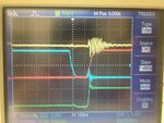
Attached is a waveform for a synchronous buck converter which, as you can see, has ringing in the output voltage (Yellow trace, AC coupled) during switching. The top two traces are gate signals, blue for low gate signal while the red for high gate signal, the bottom trace is the switching node signal. The gate driver IC I am using is LM5101 from TI and the MOSFET is BUK6218-40C,118 from NXP, I did follow the layout considerations given in the datasheet and referred to additional documents regarding how to optimize the PCB layout and placement of the DC-DC converter. Also, the dead-time between these two gate signals are programmed to be around 100ns which I think is quite sufficient, but somehow I still got this ringing issue. Can anyone help me out? thanks in advance!
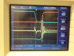
Photo Apr 05, 4 26 27 PM.jpg
 
Last edited:

By taking an AC coupled readout on the coil, it has allowed you to greatly amplify its small behavior without its DC waveform.

The ringing appears to be very fast. It is so fast that several cycles of it can fit inside your 200 nS dead time.
It might very well be at the coil's self-resonant frequency. A coil's self-resonance is an effect of the coil's Henry value combining with capacitance between its windings.
 
Thanks for your prompt reply, but I have no idea of what the coil you mentioned is, are you referring to the probe?? or something inside the scope?
 

I guess, he referred to the buck output inductor. But that's not plausible, I think. Only the commutating branch of the synchronous converter has sufficient low inductance to generate oscillations in a 100 MHz range.

In my view, it's an everydays problem with fast (MOSFET) switching circuits. The fast current peak is created when charging the output capacitance of the low side switch, additionally it might be the case that the dead time is too long and the bulk diode is conducting and adds reverse recovery charge. You'll find out by tuning the dead time and watching the waveforms.

In any case, there will be some ringing with usual switcher layouts. For really "quite" power, e.g to supply analog circuits, you'll need additional in- and output filtering of switched mode supplies and most likely separated switcher ground planes.
 
Thanks for your reply, I will try to tune the dead time based on your second suggestion. As to your first suggestion, I am wondering whether using MOSFETs with higher output capacitance helps, or modifying the layout to minimize the parasitics inductance?
 

Using MOSFETs with higher output capacitance will usually increase commutation current peaks and in case of doubt cause stronger ringing. But as resonance frequency is also changed, the effect can't be clearly predicted.

Improving the layout is most likely possible. As a first step, you have to identify the commutating current path and minimze it's absolute area. Secondly, the position and connection of the input bypass capacitors should be optimized. Finally take care that the switched current stays completely inside the converter circuit and doesn't spread over ground planes or the input supply node.
 
Without more details on the design (a picture of the layout would be great) it's hard to really tell what's up. But in my experience it's rare to see significant ringing at frequencies above 20MHz, even at the switching node. If it's in the 50MHz range, and on the output node of all places, then I would check and make sure you are probing it well (short pigtail ground connection for the probe), and that the inductor doesn't have excessive parasitic capacitance which could couple switching noise to the output.
 
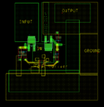
As you suggested, the layout is attached. To be honest with you, this is the third version of layout, the previous two did not work well.
As you can see, the MOSFETs, output inductor as well as input and output capacitor are placed in the top layer while the driver and associated decoupling capacitors are placed in the bottom layer. Note that some components I am using are of surface mount type and therefore I do not assign footprints for them in the layout, e.g. input and output capacitor, and output inductor.
By the way, there is also significant ringing in the switching node.
Thanks.
buck layout.PNG
 

It would be interesting though to know the position and values of the capacitors.

Also, how to you connect the output voltage probe?
 

The input and output capacitors I am using are of the same type and are electrolyte capacitor with capacitance of 220uH, rated at 100V, which I think is more than needed, I will try tomorrow to add a ceramic capacitor to see if it is able to absorb the high frequency ringing component of the output voltage.
Also, I connect the probe directly across output capacitor pins.
By the way, as you suggested me earlier to minimize the absolute area of the critical loop formed by the input capacitor, two MOSFETs, and ground, I think I did it quite well as shown in the above attached layout. Am I right??
The other thing I am not sure with is that do I really need to leave such a large area of space to the switching node?
Thanks.
 

I'm having trouble making out that layout... is green the top layer and yellow the bottom layer? Is ground only on the bottom layer then? If so then there is a great deal of stray inductance that could be eliminated.

I also can't tell where your bypass capacitors, or your inductor goes.
 

I am Sorry about the confusion, ground is mainly in the bottom layer, and also a small area in the top layer connected with bottom through via. Is there any problem with that?
And the input capacitor, output capacitor and inductor are all surface mount type, input capacitor is placed across input (labeled) and ground, output capacitor is placed across output (labeled) and ground, and the inductor is placed across the switching node (labeled) and the green rectangular area as shown in the very bottom of the top layer.
Note that the driver and associated small capacitors are placed in the bottom layer.
Thanks.
 

I got a new question while reading some documents regarding power MOSFET, my understanding is that during the turn on period, the Cgs is first charged followed by charging Cgd, while during the turn off period, the Cgs is discharged first and after a short period of turn off delay, the Cds (output capacitance) starts to be charged? Is there anything to do with the Cgd in the turn off process, or I miss something?
 

To me, it looks like a 25Mhz resonance (40ns period). Using 2*pi*f = 1/sqrt(LC), we know the capacitor and inductance values involved both need to be very small. It looks like the oscillation occurs after the bottom FET has already been off for 150ns, and immediately when the top FET is turned on. The FET itself likely represents the capacitance involved in the oscillation, and if we assume it to be ~1nF, then this makes the resonating inducance ~40nH. This is about the inductance of 3 inches of trace on a PCB. So there's your likely resonator.
 
The input and output capacitors I am using are of the same type and are electrolyte capacitor with capacitance of 220u(F), rated at 100V, which I think is more than needed, I will try tomorrow to add a ceramic capacitor to see if it is able to absorb the high frequency ringing component of the output voltage.
Also, I connect the probe directly across output capacitor pins.
You should surely use ceramic capacitors, exclusively or supplementing the electrolytic capacitors.

By the way, as you suggested me earlier to minimize the absolute area of the critical loop formed by the input capacitor, two MOSFETs, and ground, I think I did it quite well as shown in the above attached layout. Am I right??
There's still room for improvement. The ultimate low inductance layout directly stacks current and return path.
 
The inductor self-resonance energy has to be scrubbed
off by some lossy element otherwise it will recirculate
(LC tank). The tank may also consist of supply routing
inductance and decoupling caps. Playing with caps of
varying ESR (real R, not equivalent-at-frequency) can
give you a poor man's snubber circuit. I'd have a look at
the high side supply and ground with the same AC coupled
setting and be sure you're not just passing a supply-ring
to the load. The degree to which advertised inductor SRF
matches the observed tone, will indicate whether that or
some other LC is the source. I wonder about a shunt R or
series-RC parallel to the inductor, whether it could quench
ringing without too much lossiness.
 
Hi, I modified the layout but used the same components as the previous board, the waveform of which was shown in my first post. Now, I am attaching the new waveform below, the red trace is the high gate signal, the blue trace is the low gate signal, the yellow trace is the output voltage while the green trace is the switching node signal.
The ringing issue seems to be improved. On the left edge, the ringing is almost gone, but the ringing on the other edge still exists but smaller than before. One thing I notice is that when the high gate signal starts to charge, the low gate signal starts to behave strange, it also has ringing. I am wondering if it is due to the so called dV/dt induced turn on of the low MOSFET, any idea about this?
Fourth buck.jpg
 

The gate signals look more or less regular for a fast switcher. There's no dV/dt turn on detectable, it would also show at the switchung node. Some ringing isn't surprizing with gate reistors, you may also see ground bounce.
 

There are two ways to deal with the ringing noise in the output. The first is the use of a second-order post-filter (usually a small value inductor ~ 1uH, followed by several ceramic chip capacitors, usually 0.1uf paralleled with 0.01uf).
The second would be to use a snubber at your switching node.
In this instance I strongly recommend you to read TI's app note: Snubber Circuits: Theory , Design and Application by Philip C. Todd, which should available at their website. It is actually an app note written by Unitrode Corp, before they were acquired by TI.
 
The said original paper: https://www.ti.com/litv/pdf/slup100

There are probably newer seminar papers covering the same topic.

Unfortunately, the seminar papers are reorganized at TI now and then. Most should be still available but possibly hard to find. If you have the time, download the available material and make your own archives.
 
Last edited:
Status
Not open for further replies.

Similar threads

Part and Inventory Search

Welcome to EDABoard.com

Sponsor

Back
Top