Continue to Site

Welcome to EDAboard.com

Welcome to our site! EDAboard.com is an international Electronics Discussion Forum focused on EDA software, circuits, schematics, books, theory, papers, asic, pld, 8051, DSP, Network, RF, Analog Design, PCB, Service Manuals... and a whole lot more! To participate you need to register. Registration is free. Click here to register now.

Switching load between +/- voltages from 3.3V digital output

Status
Not open for further replies.

allanvv

Advanced Member level 4
Joined
Oct 23, 2010
Messages
108
Helped
14
Reputation
28
Reaction score
12
Trophy points
1,298
Location
USA
Activity points
2,078
I can easily switch a load between 0 and +15V using a mosfet. However, now I need to switch a load between -15V and 15V, at around 250kHz, from a micro out of 3.3V. Now the mosfet gate needs to have a negative voltage to be able to switch.

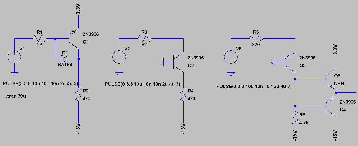
Currently I'm trying this circuit:
https://i.imgur.com/G8edT.png

When the PNP turns on, current flows through the 1k resistor to Vss which pulls the gate to voltages around Vss, allowing it to switch.

There is a relatively long delay from my logic output to the pnp turning on. In simulation the 2n3906 had 1.5us delay, while the 2n5401/mmbt5401lt1 had only 300ns delay, which is acceptable. I then tested the circuit out in real life, but found the switching delay to be 1.8us.

Should I just try a higher bandwidth transition PNP? I've never figured out how to pick what BJT's to use...
 

The gate capacitance should be known to make the switching behaviour understandable. I guess, the 2N3906 disadvantage is in it's lower B at higher collector currents (above 50 mA). Ft and capacitances are almost comparable. To make the MOSFET switching faster, it's most likely more promising to use an additional emitter follower rather than a single fast transistor. Switching the opposite edge will be the more serious problem anyway. A suitable solution requires another pnp transistor amplify the negative-going gate current.
 
I tried this arrangement and it worked well: https://i.imgur.com/VKI82.png

Unfortunately my analog design skills are mainly just trial and error based. I'm not sure I understand why connecting the bases together works well, but not if I connected Q2's base to the MCU output through a resistor or if I connected them in a Darlington configuration.
 

When reviewing the circuit and waveform, I realized that the description text had been contrary to the real operation.
There is a relatively long delay from my logic output to the pnp turning on.
The waveform reveals however, that the pnp and the MOSFET is turning on instantly, but turning off delayed. This is indicating a quite different problem. It turns out, that the gate capacitance is apparently slow, but that saturated switching causes the main problem. Adding a second transistor mainly avoids saturation of the pnp transistor. This could be achieved more effectively by a schottky diode between base and emitter.

P.S.: Besides the suggested schottky clamping technique, there are also other ways to operate the pnp transistor in non-saturated mode. Any circuit that keeps a finite Vce of at least a few 100 mV will considerably speed up it's switch-off.
 
Last edited:
It turns out, that the gate capacitance is apparently slow, but that saturated switching causes the main problem. Adding a second transistor mainly avoids saturation of the pnp transistor. This could be achieved more effectively by a schottky diode between base and emitter.

I'm not sure I understand. The base voltage goes between 2.4V to 3.3V. What would adding a schottky diode between that and 3.3V on the emitter do?

edit: I see, it limits the base voltage. It breaks the circuit, because now the diode takes all the current. Putting four in series worked though, but that seems a little hackish
 
Last edited:

I apologize for giving a wrong suggestion. I actually meaned connecting the diode between collector and base, which prevents saturation of the transistor.

Here is the schottky clamp circuit and another variant for non-saturated switching. The third circuit adds current gain to drive larger FETs with respective gate capacitance.

BAT54 is already a "large" schottky diode. You would preverably use a small one, e.g. BAS40.
 
Last edited:
Actually, I ended up just using a comparator running off +15V and -15V and pulling up its open drain to ground. Works well.
 

Status
Not open for further replies.

Similar threads

Part and Inventory Search

Welcome to EDABoard.com

Sponsor

Back
Top