Continue to Site

Welcome to EDAboard.com

Welcome to our site! EDAboard.com is an international Electronics Discussion Forum focused on EDA software, circuits, schematics, books, theory, papers, asic, pld, 8051, DSP, Network, RF, Analog Design, PCB, Service Manuals... and a whole lot more! To participate you need to register. Registration is free. Click here to register now.

Switching Current Spikes?

Status
Not open for further replies.

emaq

Member level 4
Joined
Sep 17, 2015
Messages
78
Helped
0
Reputation
0
Reaction score
1
Trophy points
1,288
Activity points
2,001
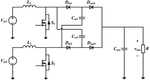
For the dc-dc converter circuit and waveforms attached, I have the following questions for the switching current spikes. The implementation detail is as under.

Switching Frequency: 100 kHz
Duty cycle: 80 %
MOSFETS are driven by MC33152 (https://www.onsemi.com/pub/Collateral/MC34152-D.PDF) with 6.5 V peak voltage.
MOSFET: IRFP260N
Average switch current: 12 A
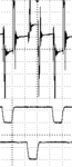
1st (top) waveform: switch S1 current
2nd waveform: switching signal for switch S1
3rd (bottom) waveform: switching signal for switch S2

1) Why these current spikes appear in the switch current? Are they usual or unusual? Any IEEE reference in past 5 years that have discussed the origin of these spikes?
2) How these current spikes can be reduced, if the actual reason is known?

BTW, the drain-source voltage waveform of switch S1 is clean (no apparent voltage spikes).
 

Attachments

  • sch.png
    sch.png
    94.2 KB · Views: 102
  • wave.png
    wave.png
    5 KB · Views: 103
Last edited:

Hi,

Most probably the spikes are caused by stray inductance because of wrong PCB layout.

I would be surprised if it is discussed in IEEE papers.

Klaus
 

Redraw your schematic such that every "wire" segment is
an inductor, each device has a capacitor from every pin
to every other node in the circuit (you may choose to
stay local, for convenience) and your resonant behaviors
will suggest themselves. Subject to appropriate scaling,
and damping and so forth.

And of course those cute little ideal-ground symbols
are in reality nothing of the sort, with power supply and
test equipment loops and parasitics all happy to sing
along.

Practically speaking, start with getting your 'scope
ground clip connection sensible and the tip / clip loop
area minimized, set your bandwidth limit to 20MHz
(if you're chopping at 100kHz, you do not need to be
looking at a 500MHz channel, 200MHz probe BW -
you'll just make yourself unhappy; save the full-BW
for when you are chasing EMI or move up to >1MHz
chopped GaN FETs, where your 'scope will be now
obsolete).

"Power Integrity" is now a thing, and you will find a
lot of this kind of stuff discussed in that context.
Have aspirin handy.
 

BTW forgot to mention that I don't have current probe (cannot afford) and measuring the current in terms of the voltage across a 0.02 Ω resistor (see the attached schematic). The resistor is a parallel combination of 5 0.1 Ω, 5 W resistors.

Hi,
Most probably the spikes are caused by stray inductance because of wrong PCB layout.

Have a look at the attached image of PCB... the red arrow point out the gate signal from MC33152 pins to the MOSFET gates. Is there anything unusual?

Practically speaking, start with getting your 'scope
ground clip connection sensible and the tip / clip loop
area minimized, set your bandwidth limit to 20MHz
(if you're chopping at 100kHz, you do not need to be
looking at a 500MHz channel, 200MHz probe BW -
you'll just make yourself unhappy; save the full-BW
for when you are chasing EMI or move up to >1MHz
chopped GaN FETs, where your 'scope will be now
obsolete).

I am already using the bandwidth limitation and noise reduction function of the DSO scope. Can I use some kind of simple RC filter in series of the probe or between drain-source terminal?

pcb.png
sch.png
 

Hi,

I recommend to read some tutorials how to design a PCB layout.
It more seems (with your PCB layout) you tried to produce oscillations instead of suppressing them.
(At least what we can see from the little snippet ... without placeplan )
* no GND plane
* no capacitors
* lengthy wiring
* capacitive coupling to gate signals

Every transistor manufacturer and gate driver manufacturer provides application notes on how to design reliable, low EMI circuits and PCB layouts. There is a good reason why they provide such material for free. So please use this kind offer.

Btw: it's not important to tell us the vaues of the used resistors, but the type:
* metal strip = good, low inductance
* wire wound = bad, high inductance
Exact type and manufacturer and/or (the link to) the datasheet...

Klaus
 

It's not completely clear which detail of the posted current waveform you consider as current spikes. Besides the three level step waveform, there are also shorter current peaks, I guess through Cmx capacitors, and finally some ringing. Only the latter is related to circuit inductance. Diode reverse recovery may also play a role.

Did you simulate the expectable circuit behavior with actual component values? How does the observed waveform differ?

Bandwidth of the current shunt is probably a problem. What are the said 0.1 ohm/5W resistors? Low inductance thick film or wire wound? Even low inductance resistors will show a high pass corner and hardly work for MHz bandwidth with two terminal connection.
 

you will always get these current spikes for fast turn on of mosfet - can be reduced by using SiC or Schottky ( up to 45V ) diodes - or by turning the fts on slower - welcome to the world of power electronics - not easy ...
 

Another bit o' switcher test trivia is, capacitance put
to the switch node will induce ringing / increase spike
amplitude. This includes 'scope probe tips. Might try a
100 ohm or 1Kohm leaded resistor wrapped around the
tip on one end, other end is now your probe tip. Taking
the Q out of the probe tip / capacitance / ground loop
segment can clean things up a lot. Of course the 100
ohms and 7pF tip would also make a 700pS time constant
and the 1K, 7nS (which might be getting too close to the
quantities of interest).
 

As others here have suggested , your top waveform in the top post is suffering from pickup...ie, noise induced into the probe.
Use a coaxial probe instead if you want...or just ignore the pickup.
To proove its pickup, connect the scope ground clip to the probe tip and also to the node of interest......youll probably still see the spikes.
 

Status
Not open for further replies.

Similar threads

Part and Inventory Search

Welcome to EDABoard.com

Sponsor

Back
Top