Continue to Site

Welcome to EDAboard.com

Welcome to our site! EDAboard.com is an international Electronics Discussion Forum focused on EDA software, circuits, schematics, books, theory, papers, asic, pld, 8051, DSP, Network, RF, Analog Design, PCB, Service Manuals... and a whole lot more! To participate you need to register. Registration is free. Click here to register now.

"Switched dumping" ??

Status
Not open for further replies.

Julian18

Full Member level 3
Joined
Apr 9, 2007
Messages
167
Helped
5
Reputation
10
Reaction score
5
Trophy points
1,298
Activity points
2,389
Hi, there
anyone can explain to me the meaning of this sentance
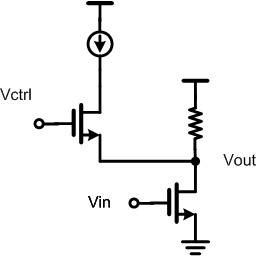
"Cascode FETs are inserted for better isolation, but also to enable switched dumping of signal currents to lower the gain"?

Thanks

Julian
 

This means that it can allow you to dump (throw away) a part of the signal current. As a result, the gain will decrease (as you purposely lower the signal current)
 

    Julian18

    Points: 2
    Helpful Answer Positive Rating
Thanks Elbadry:
but why cascode device can dump a part of the signal current? through the parasitic capacitance Cgs etc. of the cascode device?

Added after 1 minutes:

and also, why called "switched" dumping? since there is no switching action happens.
 

40_1192420885.jpg


I think what is meant is something like the above image. You can use Vctrl (which is applied on a cascode device) to do a switched dumping of current (programmable gain)
 

    Julian18

    Points: 2
    Helpful Answer Positive Rating
Hi: elbadry
Thanks for your attention, the cascode device is just a common one with its base connected to a biasing point and no switching action is occurring in this circuit, in fact, the circuit is a part of LNA.

Thanks.
 

I think it is meant that the LNA's gain can be programmed by this current-dumping action if needed
 

Status
Not open for further replies.

Part and Inventory Search

Welcome to EDABoard.com

Sponsor

Back
Top