Continue to Site

Welcome to EDAboard.com

Welcome to our site! EDAboard.com is an international Electronics Discussion Forum focused on EDA software, circuits, schematics, books, theory, papers, asic, pld, 8051, DSP, Network, RF, Analog Design, PCB, Service Manuals... and a whole lot more! To participate you need to register. Registration is free. Click here to register now.

switch capacitor filter

Status
Not open for further replies.

jianjing526

Member level 2
Joined
May 5, 2008
Messages
47
Helped
2
Reputation
4
Reaction score
2
Trophy points
1,288
Activity points
1,549
hi all,
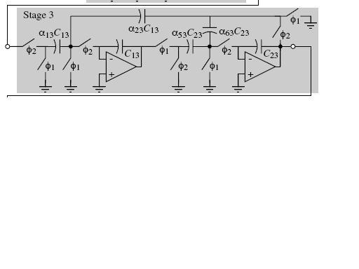
I'm designing a five-order chebyshev LPF. Three subckts cascaded to compose the filter, a one-order one and two biquads. There are five operational amplifiers. How to give out the specifications of these opamps? I'm confusing all these days!
 

It is not clear to me what you are asking for. Are you interested in opamp requirements only ? In any case, it makes sense to see your filter topology in order to see what is the role of your opamps (integrator, amplifier,....).
 

Thanks for your reply!
It's a biquad topology described in allen book with low Q. What i need to know is the specification of the opamps in the topology! Can you give some suggestions, thank you!
 

jianjing526 said:
Thanks for your reply!
It's a biquad topology described in allen book with low Q. What i need to know is the specification of the opamps in the topology! Can you give some suggestions, thank you!
It´s very easy: The opamps should be as "good" as possible.

Sorry for this silly answer, but of course one must know at least the switching frequency (clock rate) of your s/c circuit in order to recommend some opamp parameters.
Regarding the filter circuitry: there are different biquad topologies; can you describe the circuit or post a diagram because not everybody has the Allen book at hand.
 

LvW said:
jianjing526 said:
Thanks for your reply!
It's a biquad topology described in allen book with low Q. What i need to know is the specification of the opamps in the topology! Can you give some suggestions, thank you!
It´s very easy: The opamps should be as "good" as possible.

Sorry for this silly answer, but of course one must know at least the switching frequency (clock rate) of your s/c circuit in order to recommend some opamp parameters.
Regarding the filter circuitry: there are different biquad topologies; can you describe the circuit or post a diagram because not everybody has the Allen book at hand.

Oh no,i appreciate your answer. Of cource the opamp should be as "good" as possible. But if i design it as a general operational amplifier. Maybe "some high performances" is not exactly necessary! That may costs more or consumes more power. Anyway, thank you for the phase "as good as possible"!
The schematic attached below is the low Q biquad mentioned above, two poles are realized. Switching clock is 100KHz. Thank you again!
 

jianjing526 said:
....... Of cource the opamp should be as "good" as possible. But if i design it as a general operational amplifier. Maybe "some high performances" is not exactly necessary! That may costs more or consumes more power.
...................
Switching clock is 100KHz. Thank you again!

Yes, that´s the problem for each design because of some outer constraints:
Not as good as possible, but quite as good as necessary. That means that an "optimum" has to be found for each specific application. Sounds not easy.
To be specific:
As one of the most important properties your amplifier should exhibit an input impedance as high as possible to avoid parasitic decharging of the capacitors.
Regarding the output parameters, the output resistor is not so important, but the last stage should have a sufficient capability to drive the capacitive load. In many cases a two-stage cascode CMOS architecture is used with a high output impedance. Offset characteristic is not a very critical parameter. Also the gain requirements normally are not excessive.
Perhaps this helps a bit.
 

Thanks for your professional advice!
As you said, input impendence, output impedence,output drive ability and gain requirements should fulfil their needs. Maybe bandwidth should also be listed. To some extent my design satisfy those. But after a dc signal is added to the input node, nothing but zero appears in the output . Which is supposed to be the Vin*1 Since it's a low-pass component. I can't find what's wrong with my circuits. Can you give some suggestions?
By the way you are just a guy who brings me brightness in the dark! Thank you again!
 

At first, I assume you speak about the circuit as shown in your last post, right ?
Question: Did you measure (in a real circuit) or simulate the s/c structure ?
It´s really not easy to know the probable reason.
What is your amplifier supply (split or single ?).
What kind of amplifier ?
Regards
 

LvW said:
At first, I assume you speak about the circuit as shown in your last post, right ?
Question: Did you measure (in a real circuit) or simulate the s/c structure ?
It´s really not easy to know the probable reason.
What is your amplifier supply (split or single ?).
What kind of amplifier ?
Regards

Yeah, the barrier i met came from a real circuit in my last post.
Answer: I simulated in a real circuit. My amplifier is an cascaded cascode one followed by an AB output, rail to rail input and output. It's powered by a single dc voltage source. Thanks!
 

I think, you have to follow the classical way of detecting errors:
1.) Check power supplies and - as a desired result - the bias conditions of all active devices. Is it possible for any signal to swing around the bias point ?
2.) Check if the switches are activitated by the clock signal.
3) Check the signal path from the beginning - in your case after the first switch and so on.
Good luck.
 

Status
Not open for further replies.

Similar threads

Part and Inventory Search

Welcome to EDABoard.com

Sponsor

Back
Top