Continue to Site

Welcome to EDAboard.com

Welcome to our site! EDAboard.com is an international Electronics Discussion Forum focused on EDA software, circuits, schematics, books, theory, papers, asic, pld, 8051, DSP, Network, RF, Analog Design, PCB, Service Manuals... and a whole lot more! To participate you need to register. Registration is free. Click here to register now.

Suggestion required for H-Bridge circuit

Status
Not open for further replies.

xyz9915

Member level 4
Joined
May 14, 2007
Messages
74
Helped
2
Reputation
4
Reaction score
2
Trophy points
1,288
Location
Pakistan
Activity points
1,817
h bridge circuit

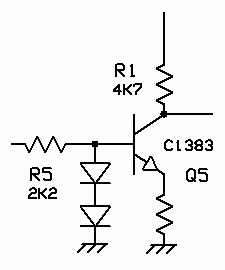
Hi! The attached file is a schematic of 50 Hz H-Bridge which I want Ito use in the final stage of an inverter. In this respect please help me either any modification in the circuit is required? the power of inverter is 500 Watts.
 

The high side drive circuit probably cant' work that way. When Q5 or Q7 are switched on, part of the load current is flowing through the transistors for some time. I don't now about their power capability, the type is unknown to me, but an effective current limiting mechanism should be present to my opinion. Switch-on operation is rather slow due to 4K7 resistors (I guess 5 - 10 us), but this may be O.K. for 50 Hz operation. Paralleling MOSFET without individual gate resistors generally raises a risk a RF oscillations during switch on-ramp.
 

FvM said:
The high side drive circuit probably cant' work that way. When Q5 or Q7 are switched on, part of the load current is flowing through the transistors for some time.

Correct. MOSFET driving voltage is referenced between gate to source.
IRF840 is an 500V 8A continuous drain current, >8V Vgs


I don't now about their power capability, the type is unknown to me, but an effective current limiting mechanism should be present to my opinion. Switch-on operation is rather slow due to 4K7 resistors (I guess 5 - 10 us), but this may be O.K. for 50 Hz operation. Paralleling MOSFET without individual gate resistors generally raises a risk a RF oscillations during switch on-ramp.
 

The circuit may be near to a functional design, but some changes are necessary. At least current limiting for the high side drivers as shown below would be necessary, provided the type has the necessary > 300 V Uce capability. Another problem is in initial charging the bootstrap capacitors, this may require separate control of high-and low-side drivers. Also it must be assured, that the bootstrap voltage can't drop below a minimum value of e. g. 8 V. All in all it may be advisable to use integrated drivers as IRF 2110 instead, they achieve fast switching, so the switching losses would be reduced.

0_1209921271.gif
 

Thanks for helping, the current limiting for the high side drivers is changed to the picture shown. The transistor type changed from C1383 to MJE13005 (400V/4Amp). The initial charging the bootstrap capacitors, which requires separate control of high-and low-side drivers. so please suggest modified design because IRF 2110 is not commonly available and it is also very expensive chip.
 

It's not expensive in Germany, but I see that it may have different pricing or be unavailable at your location. To my opinion, a simple start-up scheme would be to activate both low side switches first with high side switches off to load the bootstrap circuit and start normal operation then. This would require 4 separate drive signals. I don't know how you intend to generate the drive signals with a dead time, if a microprocessor would be used, it's most simple to have 4 separate outputs.

Generally, it's advisable to start test operation with a current limited HV supply to reduce the danger of transistor damage with incorrect drive signals or drive circuit operating badly.
 

Status
Not open for further replies.

Part and Inventory Search

Welcome to EDABoard.com

Sponsor

Back
Top