Continue to Site

Welcome to EDAboard.com

Welcome to our site! EDAboard.com is an international Electronics Discussion Forum focused on EDA software, circuits, schematics, books, theory, papers, asic, pld, 8051, DSP, Network, RF, Analog Design, PCB, Service Manuals... and a whole lot more! To participate you need to register. Registration is free. Click here to register now.

Suggestion for high speed class AB op-amp

Status
Not open for further replies.

Junus2012

Advanced Member level 5
Joined
Jan 9, 2012
Messages
1,552
Helped
47
Reputation
98
Reaction score
53
Trophy points
1,328
Location
Italy
Activity points
15,235
Dear friends,

I mostly use the class AB circuit shown below for most of my design, it is like butter and bread for me, but since now I am targetting a GBW = 250 MHz, I am finding difficulty to get this value from this circuit. I cant ignore the fact the buffered op-amp is limited in speed due to the compensation capacitor so I am trying to increase the differential biasing current, increasing the output current (M11 & M10) to push away the non-dominant pole that helps in reducing CC, I killed myself to reach GBW = 100 MB with PM = 55.

I like the circuits based on folded-cascode core because it is easy to implement rail to rail input stage.

So I am not sure if there is a better buffer circuit to use ? or another possibility to extend the GBW of this circuit.

I am using the 0.35 µm technology.
The intended application is for active LPF design.

Thank you
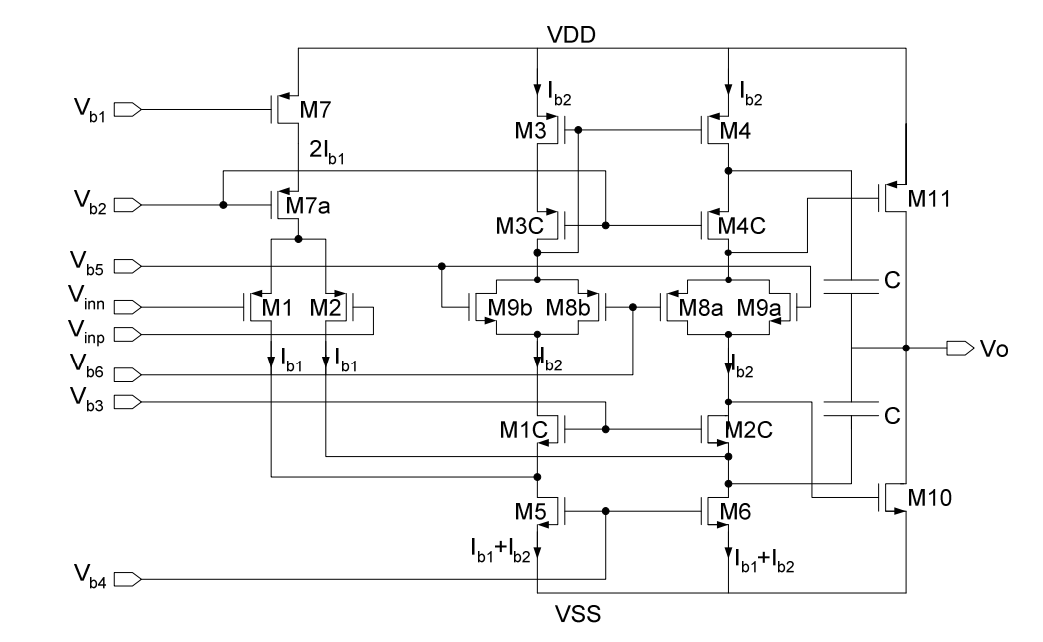
classab.PNG
 

it is in the range of 20 pF which invloves the filter feedback capacitor plus the input capacitor from the next stage
 

According to me it is not the compensation caps that limit the speed as it is the many non-dominat poles that you have in that classical class AB topology. If you have enough headroom at the output, maybe you can think of using a regular two stage Miller compensated amplifier with source follower buffer. There won't be anything faster than the regular two stage opamp. Perhaps you can use the second stage to drive your resistive and capacitive , and thus compromise on the 2nd stg gain and have most of your gain in the first stage, which can be folded or telescopic cascode.
 
Assuming 20pF load and 5MHz f_c (so SR>38V/µs) and UGF 250MHz, you don't need class AB.
Try nmos input miller like this:
miller_nmos.png

multipliers in figure are number of fingers simply.
Input pair: 12×12/0.35
NMOS sources: 5/0.35 per 100µA
PMOS sources 10/0.35 per 100µA.

With this numbers:
1. output stage current is 20mA
2. tail current is 2.4mA
3. Input stage gm ≈ 10mS
4. output stage gm ≈ 112mS
5. Input cap is ≈ 0.8pF
6. 2nd stage cap ≈ 7pF
7. non-dominant pole ≈ 420MHz
8. dominant pole ≈ 27kHz
9 UGF ≈ 250MHz
10. DC Gain ≈ 80²/4 ≈ 1600 → ≈64 dB
11. SR ≈ 184V/µs
12. offset ≈ 2mV/sigma
13. DC points should be OK (VGS of pmos ≈1.1V, nmos ≈0.85V and input pair ≈ 0.75)
above are my hand calculations, so don't guarantee are OK.

However, one question arise to me during this calculations.
AAF is followed by ADC. 20pF seems like you would like to use capacitive SAR ADC. I doubt, in this technology you can achieve 12bit capacitive SAR with sampling higher than 10MS/s.
Have you such ADC?
Maybe your output cap is overestimated by factor 10 (12 bit pipeline will need ca 2pF).
 
Last edited:
Dear Dominik and Suta,

Thank you very much for your very helpful reply,

Dear Dominik and Suta You both suggested not to use class AB stage, while it is assumed the class AB to be more power-efficient? or do you suggest that because the static current is already high enough so no need to increase it further by the class AB operation? or maybe another reason.

To answer Dominik questions,

The intended SAR to use is 12-bit Pipeline, but I think when we calculate the CL we should consider the capacitors in the feedback of the filter, isn't it?

Regarding your suggested two-stage op-amp, I see you are using the minimum channel length, is it possible? I only use the minimum channel length in digital design,

Also for me I never had a current value like 20 mA or 2.4 mA for biasing the amplifier, you can say I have no experience but would such value accepted in IC community? especially I will convert it to fully differential amplifier where it will about have twice the power.

I found TLV3544-Q from TexasInstrument, it is stated that consumes 5.2 mA to reach 250 MHz, of course, I can not compare myself to them but only an idea, they are using class-AB CMOS op-amp


I will try your circuit after your comments

Thank you very much once again especially for the hand calculations

Regards
 

Did you expect drive such cap with no current? Notice, mentioned TI opamp has 200MHz UGF at 5.6pF, so it's current consumption can be lowered to this 5mA. With 20pF 24mA is what you should expect. Notice also, that TI opamp uses class-AB to ensure more than 100mA driving capability, which you don't need.

The common FoM for two stage opamp is 375MHzpF/mA achievable for moderate inversion bias. In 0.35 you can't go to moderate inversion to achieve sub-GHz bandwidth, so expected FoM drop to ca 200MHzpF/mA. This number fit to 25mA to meet your spec.

It might be possible to get 250MHz with 2mA fully differential design but with fancy architecture only (which I will not share).

Regarding load cap. Yes, feedback cap should be included, but I believe this cap is below 1pF, isn't it? So, in total it would be ca 3-5 pF. At least for 10bit pipeline we used ca 500fF caps, so 12 bit might have 4 times bigger only.
--- Updated ---

Regarding your suggested two-stage op-amp, I see you are using the minimum channel length, is it possible? I only use the minimum channel length in digital design
It is the only way to do it.
--- Updated ---

Also for me I never had a current value like 20 mA or 2.4 mA for biasing the amplifier, you can say I have no experience but would such value accepted in IC community? especially I will convert it to fully differential amplifier where it will about have twice the power.
Look on power consumption of microprocessors, they are counted in hundreds of watts. Look on TX power in wifi or 5G. Again it is in watts. Miliamps are not unusual numbers.

About doubling current in fully differential, i can only say "sorry Winnetou".
 
Last edited:
Thank you Dominik once again

It might be possible to get 250MHz with 2mA fully differential design but with fancy architecture only (which I will not share).

will it be possible to share similar one :)

I found this paper


Regarding load cap. Yes, feedback cap should be included, but I believe this cap is below 1pF, isn't it? So, in total it would be ca 3-5 pF. At least for 10bit pipeline we used ca 500fF caps, so 12 bit might have 4 times bigger only.

I use 5 PF

Any way this makes the calculation no more than 10 pF let me say.
 

I use 5 PF
In filter feedback? So another cap in filter is 50pF? Nevertheless, I don't believe you need more than 300fF in filter feedback. You don't add gain in AAF and your noise constraints for sure are not so strict. Or they are?
 
In filter feedback? So another cap in filter is 50pF? Nevertheless, I don't believe you need more than 300fF in filter feedback. You don't add gain in AAF and your noise constraints for sure are not so strict. Or they are?

Dear Dominik,

Thank you for the reply

Consider the circuit as an example of the Sallen-Key filter below, suppose that C1 = C2 = 5 pF. It is recommended not to use a capacitr less than 10 PF otherwise the op-amp parasitic will dominate it and shift the filter frequency, that what told by TexasInstrument filter design procedure,

So it is 5 pF not 50 pF.

For the circuit below CL (equivelant) = C1 || C2 + CL
= 5 pF+ 5 pF + 2 pF = 12 pF.

sallen_key.png


Please see this similar op-amp also from TexasInstrument and tested with 5.6 pF but in the filter implementation they used 150 pF and mostly common people use a capacitor in term of nF without even using isolation resistor (in discrete design),

Note: If the CL = 5.6 pF this means that CC is in range if 1.5 pF


By anyway I will be more have if I relax the design by reducing the values of the capacitors if it is possible
 

Consider the circuit as an example of the Sallen-Key filter below, suppose that C1 = C2 = 5 pF.
Don't use Salen-Key topology.

Example MFB:
Screenshot_20200828-185406_Chrome.jpg

C1 is nicely isolated from opamp output, feedback is 300fF. You don't need more.

It is recommended not to use a capacitr less than 10 PF otherwise the op-amp parasitic will dominate it and shift the filter frequency, that what told by TexasInstrument filter design procedure,
In discrete design is hard to find good Capacitor in range of single pF, and discrete opamp has terminal capacitance in order of single pF due to package, pads, esd, etc.

In IC you are connecting everything directly.

So, please read datasheets with proper context or don't read at all (over knowledge harms).
 

    Junus2012

    Points: 2
    Helpful Answer Positive Rating
Dear Dominik

I am very thankful to you

I still remember your suggestion of not using the Sallen-Key,
For a fully-differential amplifier, MFB is so straightforward applied.

So I see for you using Cap less than 10 pF is ok, I will follow your suggestion

I will tell you why I am shifting to Sallen-Key,

Since my task is to have tunable filter by using MOS resistor, with MFB to tune the fc I have to be alwys sure about the gain and Q, hence all resistors have to be tuned equally,

In sallen-key topology, if I select C1 = C2 and R1 = R2 then I can control the Q, AV, fc separately and most important less error I have when varying fc

in case if I have fixed design, definitely MFB should be my first choice
--- Updated ---

By the way, I am not happy with sallen-key filter cause it is non-inverting amplifier imposing the need of rail-to-rail input stage, which will be counted for power as well
 
Last edited:

In MFB you can set R2=4R1=4R3 and tune resistor value by single control signal as well.

Salen-Key with opamp having common source output stage will not work. However, I see you need to discover it by yourself.

Since my task is to have tunable filter by using MOS resistor,

It will not work, unless all MOS resistors will have the same Vds. As long as you will use stages with unity gain and high swing of signal you will not ensure this condition.
But again. Good luck, I see you need to discover it by yourself.
 
Dear Dominik

I am not going to say goodbye early to you :)

I believe on your arguments, I would follow it exactly, it is only matter of satisfying my boss demands, if it is up-to me I will never use the MOS resistor, it has poor non-linearity thus suits only small signals like for bio application, beside controlling is not straightforward predicted, I am aware of these things also had a discussion on it, but my group leader insists on it, indeed he is attracted to this paper:


https://link.springer.com/article/10.1007/s10470-011-9640-7

He wants to use the circuit in Impedance spectroscopy with range from several Hz to 5 MHz, that is all what I know, have no idea even what the hell is Impedance spectroscopy. But I know he has amplifier before the filter that is why I expecting the input signal to the filter is not small.


back to the full-diff MFB, and please refer to the below circuit (consider only the 2nd order and ignore the passive added stage)


MFB.PNG


, how it will be possible to have fc independent on Q and gain (K) when they share all components (except for R1) ?

I would say in non-tunable and since fc is not depending on R1 then one can use to adjust the gain and compensate for Q change.

For tunable filter we need to shift R1 as well to keep constant gain ratio that is not changing by selected fc.

So you see criteria for fixed corner filter is much easier and different for tunable one.


I hope I don't make you feeling boring,
Your experience helped me a lot

Thank you once again
 

I know this implementation. It might be tricky due to diode leakage and swing is limited to +/-0.3V. So, you will use only 20% of available swing. Also body effect in source follower might affect performance.

what the hell is Impedance spectroscopy.
It is one of the method in material science.

how it will be possible to have fc independent on Q and gain (K) when they share all components (except for R1) ?

I would say in non-tunable and since fc is not depending on R1 then one can use to adjust the gain and compensate for Q change.

For tunable filter we need to shift R1 as well to keep constant gain ratio that is not changing by selected fc.
If you create one tunable unit and use it to create all resistors, you will be able to trim cut-off frequency and keeping Q factor and gain constant. However, if you want to vary all filter parameters you will suffer for old proverb "if sthing is for everything then is useless" and need to trim every component independently.

Nevertheless, Salen-Key is killed by finite opamp output impedance (it might be overcame by use of another buffer).

So wide range of cut-off frequencies might force you to use bank of caps and limit maximum resistance due to noises.
Mentioned in linked article (there is also a book of those two guys) pseudo resistor implementation might be not suitable for low resistance values.

Once again, good luck.
 

    Junus2012

    Points: 2
    Helpful Answer Positive Rating
Dear Dominik,

Thank you once again

you create one tunable unit and use it to create all resistors, you will be able to trim cut-off frequency and keeping Q factor and gain constant.

Whih combination setup leads to these properties? I tried several assumptions on the transfer function formula to make them independent but concluded that is not possible. Which values ratios satisfy this condition ?


So wide range of cut-off frequencies might force you to use bank of caps and limit maximum resistance due to noises.
Mentioned in linked article (there is also a book of those two guys) pseudo resistor implementation might be not suitable for low resistance values.

Yes I have the book of those guys "Extreme Low Power Mixed Signal IC Design"

Using Bank of capacitors will bring me back to the problem of having a high capacitive load, one of the reasons I assumed C feedback of 10 pF is to minimize the resistor size at low frequencies, but I and you had a conflict on why not using small capacitor value of less than 1 pF :) :)

To be honest with you and myself, after you guys helped me and after reading many advanced articles from TexasInstrument and other big companies I realized many things that I shouldn't know :)...... Integrated Active filters are very power-hungry that makes them not suitable for high fc, and for very small fc it imposes a problem of components size. To overcome this proble and for the purpose of tunability, MOS based resistors are suggested. However, the linearity that we are proud of it from active filter are going to be lost.

So if I would compare MOS-C filter with gm-C filter, I think gm-C win with honour, although I didn't study the latter yet but people happy of its tunability and it is requiring GBW that is equal to the fc . Yes I believe that gm-C filter is not that linear as it is based on open-loop integrator, but can be sufficient for 8-bit resolution while I am really not sure if 8 bit can be reached in MOS-C filter.

I have read many articles about high performance MOS-C, but I would say all authors shows the good side of it and hiding the roubles, that is why I found in TexasInstruments or Analog Devices most of the real and practical truth in their rich documentations
 

Whih combination setup leads to these properties? I tried several assumptions on the transfer function formula to make them independent but concluded that is not possible. Which values ratios satisfy this condition ?
I might be wrong of course. What I remember when I designed such filter last time, R1=R3=Ru and R2=4Ru and Ru was trimable. Gain was set by ratio of R2/R1=4 independent to Ru value. Q-factor was set also by ratio of proper RCs fixed by trimable units.

Integrated Active filters are very power-hungry that makes them not suitable for high fc
If you study topic deeply you find this statement false. Active RC filters are the only choice in many applications. Also, in case of set lower fc you will not need so high GBW. So opamp power can be scaled as well. In very high frequencies it is a problem. But RF is a problem itself.

So if I would compare MOS-C filter with gm-C filter, I think gm-C win with honour
With gm-C is not possible to get more than 50dB attenuation (usually it is 40dB). Swing is limited to input pairs linearity (100mV-200mV maybe), sacrificing the noises. They are better in very high frequency applications (fc>100MHz) but still with moderate parameters.
If you look on power consumption, it is very similar between various filter architecture and is in range of mW/pole/MHz. SSF and FVF or triode MOSFETs based filters can go lower (ca 10×) with power but they are suffers for other issues.
Class-C/D, inverter-latch based transconductors and ring-oscilator amplifiers achieves better FoMs (in power vs DR vs BW) but are aggressive, sensitive and poor in other properties.

Design is like squeezing the balloon.
 

    Junus2012

    Points: 2
    Helpful Answer Positive Rating
Thank you Dominik,

It was wonderful discussion with you today, I will update you with the result of the amplifier you suggested me

Just for clarity, I was complaining of the active RC at very low frequency due to the need of large RC value, despite the fact as you said they requires less GBW and so less power,
Yes I forgot also that gm-c filter is a problematic at low frequency as well since RC = 1 / gm C, which means very high R is as same as very small gm, not that simple thing, I saw one paper of a designer trying to kill the gm by using mirror OTA with mirror ratio very less than one, so he stacked a lot of series transistors at the output.

Just to add one thing, gm-c filter with simple linearization techniques could achieved linearity about 60 dB, I believe you aware of the famous authors Sansen and Martinez, they implemented a good linearization circuit for gm-c filter wiht about vin = 2 Vp-p.

file:///C:/Users/Senan/Downloads/Chapter_19.pdf


Thank you once again
I wish you nice weekend

Best Regards
 
Last edited:

Dear Dominik

I tried to make the simulation of the circuit suggested in #5
but the tail transistor is not going in to saturation and the result is far from suggested

maybe I am taking the ratios wrong, so could you please refer to the exact ratio for each transistor, and I will divide the number of gates myself
--- Updated ---

By the way Dominik,

I see for high speed op-amp commonly to have low DC gain like in terms of 60s or even 50s, why then people try have high DC when the GBW is more important than having high DC gain

even with op-amp having high DC it will soon drop and bode plot of high DC gain and small DC gain op-amp will be identical (if they have the same GBW) at high signal frequency
 
Last edited:

1. Tail current NMOS: Wtot=120µm, Wfinger=5µm, NF=24, L=0.35µm, Id=2.4mA, Vdssat≈335mV, Vgs≈0.8V
2. Input Pair: Wtot=144µm, Wfinger=12µm, NF=12, L=0.35µm, Id=1.2mA, Vdssat≈240mV, Vgs≈0.7V
3. PMOS Current mirror in 1st Stage: Wtot=120µm, Wfinger=10µm, NF=12, L=0.35µm, Id=1.2mA, Vdssat≈0.4V, Vgs≈1.1V
4. NMOS in 2nd stage: Wtot=1000µm, Wfinger=5µm, NF=200, L=0.35µm, Id=20mA, Vdssat≈335mV, Vgs≈0.8V
5. PMOS in 2nd stage Wtot=2000µm, Wfinger=10µm, NF=200, L=0.35µm, Id=20mA, Vdssat≈0.4V, Vgs≈1.1V
In 2nd stage, current might be 5% higher (so Id≈21mA) due to 0.5V higher Vds (with 1.65V common mode and 3.3V supply)
I checked calculations and they seems to be OK (inversion level for input pair is ≈10, NMOS sources ≈24 and PMOS'es ≈35).
With 1.65V provided to OPAMP input, Vds of tail current should be ca 0.9V so it should ensure 0.5V of margin for saturation.

Bias amplifier from NMOS current mirror with 100µA ref current and diode connected NMOS Wtot=Wfinger=5µm, NF=1, L=0.35µm.


Regarding gain question. I think, in one post some time ago I tried to explain it.
Everything depends to application. High gain is needed for high accuracy. If we consider 40dB OL gain (100V/V) and feedback system with 1V provided for non-inverting input. The opamp will copy this 1V to inverting input with accuracy of ≈1% (instead of 1V you will see 0.99V or 1.01V). So, for high accuracy circuits like D/A or A/D converters (eg. pipeline ADC), to meet certain level accuracy you need to ensure enough gain - for example, for 10bit pipeline, OPAMP in 1st stage MDAC has to have at least 4×2^10 V/V =4096V/V → 72.3dB. Of course for fast ADC, such OPAMP need both high gain and high UGF. In bandgap circuit high gain might be enough with no strict constraint for UGF.

In contrary, for some preamplifiers, very high UGF is more important due to PSRR requirements (PSRR is ratio of output impedance to impedance seen from VDD, so as long as feedback loop works, Zout is low, even if preamp loop bandwidth is narrow), while moderate (i would say 40-60dB) gain is sufficient for other spec.
 
Last edited:
Status
Not open for further replies.

Part and Inventory Search

Welcome to EDABoard.com

Sponsor

Back
Top