Continue to Site

Welcome to EDAboard.com

Welcome to our site! EDAboard.com is an international Electronics Discussion Forum focused on EDA software, circuits, schematics, books, theory, papers, asic, pld, 8051, DSP, Network, RF, Analog Design, PCB, Service Manuals... and a whole lot more! To participate you need to register. Registration is free. Click here to register now.

subtract contact (subc) in 0.13um process ibm8rf kit

Status
Not open for further replies.

Alvaro Camacho Mora

Newbie level 4
Joined
Apr 19, 2015
Messages
5
Helped
0
Reputation
0
Reaction score
0
Trophy points
1
Activity points
37
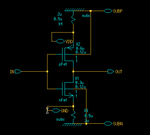
Hello! I need help I'm new in 0.13 um process using ibm8rf kit. In my first circuit and layout, I made a logic inverter. However this inverter working successfully in the schematic, but in the layout I have a big problems because the subtract mask don't connect with the transistor and I don't know if this form of connection is correct. In the adjust file, I show an image of my schematic. I use mentor graphics.
Thanks.
 

Attachments

  • inverter.png
    inverter.png
    16.7 KB · Views: 125

Hi,

Bulk for NFET/NMOS should be connected to GND. Bulk for PFET/PMOS should be connected to VDD. I don't think you really need that resistors.

INVERTER.png
 

subc is used only to connect bulk of nfets to ground. pfets has bulk connected directly to the vdd or source.
 

Thanks. Yes, I understand this. But, when I want to create the layout, I pressed in "Auto peak and place" and then I create the connections between the transistors. The connections between the bulk and vdd/gnd don't be create. Next I have problems in LVS because the bulk isn't connect, appear one black box. And other question, in the schematic, the connections in nfet with subc, is ok?

Thanks.
 

Status
Not open for further replies.

Part and Inventory Search

Welcome to EDABoard.com

Sponsor

Back
Top