Continue to Site

Welcome to EDAboard.com

Welcome to our site! EDAboard.com is an international Electronics Discussion Forum focused on EDA software, circuits, schematics, books, theory, papers, asic, pld, 8051, DSP, Network, RF, Analog Design, PCB, Service Manuals... and a whole lot more! To participate you need to register. Registration is free. Click here to register now.

substrate definition

Status
Not open for further replies.

Coust

Member level 2
Joined
Oct 1, 2013
Messages
48
Helped
1
Reputation
2
Reaction score
1
Trophy points
8
Activity points
472
substrate definition in ADS 2011

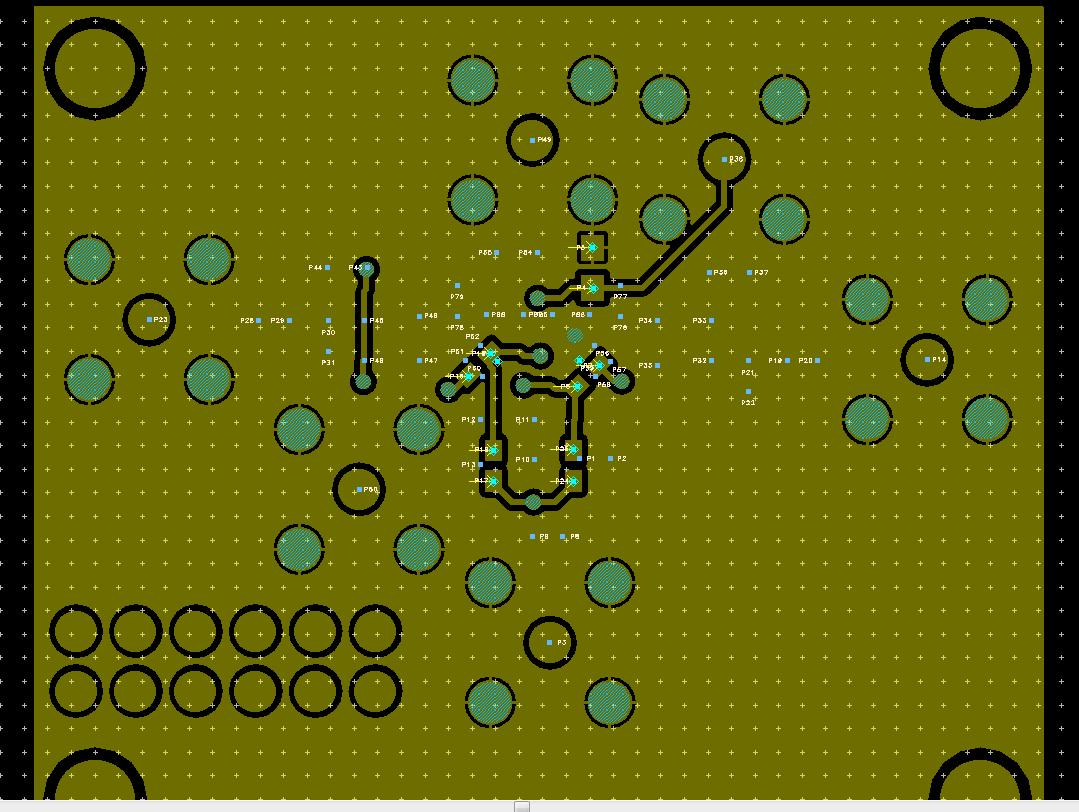
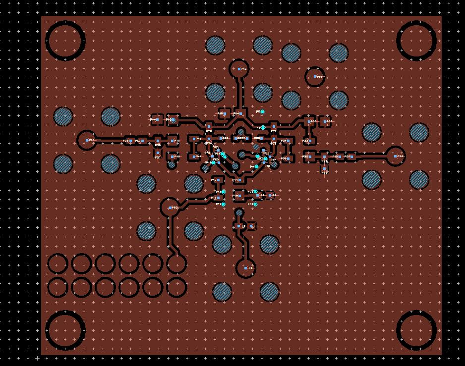
Hello there I'm looking to set a substrate in ADS2011 to simulate a PCB design. The problem I face is that I have a 2 metal layer PCB: cond1 dielectric cond 2 because I have path in both sides of the board. I would like to get a EMmodel to simulate in schematic but it seems that is not working as It should do and I think that the problem is the GND definition. If I have this cond1 dielectric cond 2 where (and how) do I have to set the GND?

Ty very much

Substrate I have right now:
subs.jpg
 
Last edited:

The basic idea of your substrate model is correct, but there is some detail problem. In the status line at the bottom, you see that the substrate editor complains about an error. This might be something trivial, but you need to fix this.
 

I checked it and it is correct, probably it was something that I changed before I took the picture. How do I set the GND?
This is what I have:


Do I have to set the GND using the symbol or a pin? Or do I have to set it in the schematic?

Ty!
 

Do I have to set the GND using the symbol or a pin? Or do I have to set it in the schematic?

I don't understand your question.

You have pins on the GND layer, and from what I see, you have one GND layer pin for every signal layer pin. This looks good. You can now create differential ports in the port setup, so that the GND layer pin is the (-) terminal and the signal layer pin is the (+) terminal.

If you leave all the pins as is, with no explicit (-) terminal, you might get warning about unphysical results. That unphysical result warning isn't real, because results get physical after properly combining the signals and grounds. The use of the look-alike symbol is
somewhat difficult if you have overlapping pins on different layers that you all need to connect. You might shift them just a little bit.
 

Sorry, I'm not a native speaker and my english is not as good as it should be. I will try to explain what I said before. I mean that I have 2 pins for every SMD element. There are few components that are grounded, such as decoupling capacitors. So I have 1 pin in the signal path and another one in the ground:


The question is: Do I have to create differencial ports and assign the + terminal to P36 and the - terminal to P37? If it's correct, What do I do with P77, P76, P34...etc.? Do I have to assign + terminal for each port and the - terminal to P37 to set the same ground?
I have plenty of this capacitors so I have different pins attached to my ground layer. Do I have to delete all of the pins except P37 (for example) and then set the + terminal to each pin and the - terminal to P37? Or is it better to have a few GND ports?

Ty very much volker!
 

The question is: Do I have to create differencial ports and assign the + terminal to P36 and the - terminal to P37?

I vote against that, because it only works for pure series element. If you attach S2P data for R,L,C these usually have some shunt parasitics to ground as well. If you use a differential port with (+) on one pad and (-) on the other pad, you will loose that shunt current.

https://muehlhaus.com/support/ads-application-notes/momentum-port-global-ground-or-differential

Only for pure series elements, with no shunt parasitics, it is ok. Then, you don't need the pins under the SMD pads on the GND layer.

I have plenty of this capacitors so I have different pins attached to my ground layer. Do I have to delete all of the pins except P37 (for example) and then set the + terminal to each pin and the - terminal to P37? Or is it better to have a few GND ports?

Most of this answered above? You need pins of the GND layer where you have physical current flow to/from that layer. So at least you need them at the input and output connections, and all deviced where current flows to/from the GND layer.
 

Ok, I understand that but my problem is that I don't have an infinite ground to set the - reference of my ports. I don't know how ADS can handle that and where it sets the GND reference. This is the reason I think that I need diferencial ports instead of grounded ports.
 

I am aware of that, and you don't need it. Maybe you misunderstood some part of my answer?

Ok, I understand that but my problem is that I don't have an infinite ground to set the - reference of my ports.

If there is no infinite ground, and you have not assigned an explicit (-) pin, Momentum will use that magic "ground at infinity", as described in the Momentum documentation. This will results in S-parameters that are ONLY physical after connecting the devices.

I don't know how ADS can handle that and where it sets the GND reference. This is the reason I think that I need diferencial ports instead of grounded ports.

Yes, this is what I suggested above. But you need to use the differential ports in a different way. For each pad, you have the signal pin on the pad (+) and the reference pin (-) on the GND layer below the pad. This is the best, universal method because you have true 2-port connection for the devices.

All this port stuff is simple if you think of the EM model and ports as paths where signal and return currents flow. With your port defintions, you must enable that current flow in the locations where it physically makes sense.
 

Ok, I think that I got it. I need those differential pins where I have a real current exchange and the - pin has to be in the layer below the + pin. But, what about the other pins such as P34? There is not a physical connexion with the ground. How do I have to set these pins?
 

But, what about the other pins such as P34? There is not a physical connexion with the ground. How do I have to set these pins?

From what I see above in post #5, this is a pin on the component pad? If there is some ground below, I would assign the (-) terminal to that ground below. If there is no ground below, you can [A] use (+) and (-) between the two pads of that component, resulting in one port for that component or leave the (-) assigned to that magic ground at infinity (my post #4) and then have two ports so that you connect the component between these two ports.
 

Status
Not open for further replies.

Part and Inventory Search

Welcome to EDABoard.com

Sponsor

Back
Top