Continue to Site

Welcome to EDAboard.com

Welcome to our site! EDAboard.com is an international Electronics Discussion Forum focused on EDA software, circuits, schematics, books, theory, papers, asic, pld, 8051, DSP, Network, RF, Analog Design, PCB, Service Manuals... and a whole lot more! To participate you need to register. Registration is free. Click here to register now.

[SOLVED] "subc" terminal = substrate contact. (IBM process). LVS error.

Status
Not open for further replies.

palmeiras

Full Member level 6
Joined
Feb 22, 2010
Messages
375
Helped
61
Reputation
122
Reaction score
50
Trophy points
1,308
Location
South America
Activity points
4,199
Hi guys!

Have anybody faced this problem before?
I´ve read some other threads but I didn’t get the solution yet.

I´m using IBM technology and it has the substrate contact "subc".

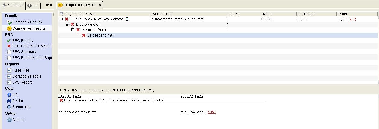
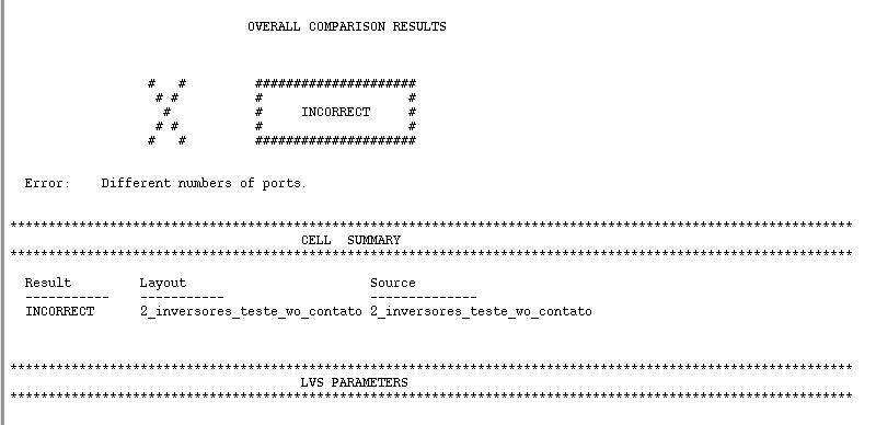
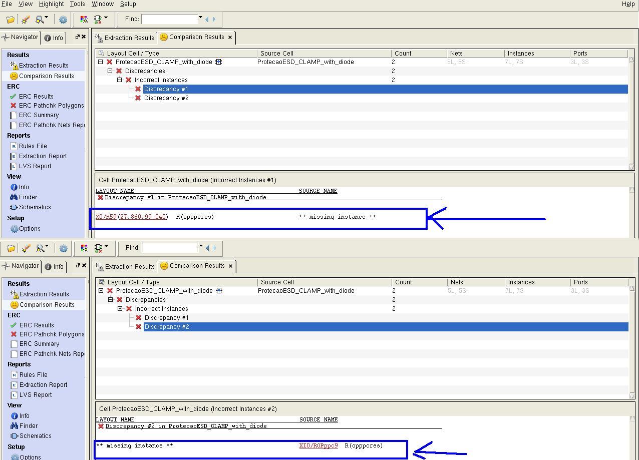
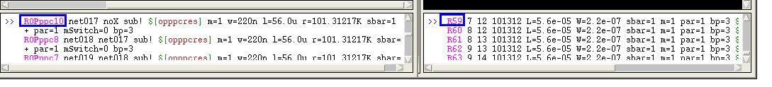
I´ve designed an inverter and it does not present any error of DRC and LVS (100% clean). However when I´ve designed another cell composed by two inverters, the LVS does not pass. Why?
Because in the layout: all GND pins and subc contacts are connected together. But this connection is not possible in the schematic when each inverter cell has its own subc, and I cannot connect these substrate contacts in parallel.
Does anyone have a recommendation to overcome this issue?

Thanks in advance,
 

Hi palmeiras

I have worked with IBM kits for a few years so I am quite familiar with the subc concept, only caveat is that I do not use assura but calibre
there are several solution to dealing with subc's
- ignore them by using GRLOGIC layer that suppresses the extraction of subc (and unexpectedly cuts the substrate in Calibre)
- use them with explicit pins
- use them with inherited connections

Since you are designing all your cell I would recommend using one the last two options.

To understand what went wrong in your case you probably need to show us what you did in schematic and layout, there is no reason why you cannot connect GND to subc in both inverters in the schematic to get a clean LVS...
 
  • Like
Reactions: palmeiras

    V

    Points: 2
    Helpful Answer Positive Rating

    palmeiras

    Points: 2
    Helpful Answer Positive Rating
From your description i understand that you have the following situation :

1.Hierchical schematic with two inverters
2.Each inverter has its own subc component at the schematic side

Up to here everything sounds correct if this is your case.

Assuming the above as given do the following for each inverter cell :

--SCHEMATIC SIDE :

Press q button to access the properties of the subc component and you will see an option "LVS MARKER".This should be OFF.

--LAYOUT SIDE :

1.Select all subc contacts and their LVS MARKER option here should be ON.
2.Delete the subc pin that came into layout XL with update components and nets.
3.Connect with metal (usually M1) all the subc rings to the VSS line

---------------------------------------------------------------------------------------------------------------

For the Top Level schematic with the two inverters :

1.You should NOT have subc component.
2.There slould be only one pin with global VSS

At the layout side just connect with metal the two individual VSS lines of the 2 inverters and you are done.

Finally after the above your LVS should be clean.

If not come back here and show me the screenshot of the exact LVS error and the exact schematic and layout screenshots to assist you further.
 
  • Like
Reactions: palmeiras

    V

    Points: 2
    Helpful Answer Positive Rating

    palmeiras

    Points: 2
    Helpful Answer Positive Rating
Hi dgnani and jimito13,

Thanks for your replies. I´m sorry for the delay.

Last week I´ve figured out a way to solve this issue.
As dgnani has suggested, If inherited connections are used, the LVS with ASSURA has success. But the problem still continues when using Calibre.
Thanks jimito for your suggestion, but the problem is that the subc contact does not have “LVS MARKER” in this PDK. I remember that the old IBM technology that we´ve worked had this option.

Do you have a suggestion to make the LVS clean when using Calibre? How do you use the GRLOGIC layer?

By the way, I have set the Calibre configuration as described bellow:
NO_SUBC_IN_GRLOGIC: TRUE

Obs: it is attached the caliber error messages.

Thanks in advance.


I have experience with ibm 0.13 and Calibre is somewhat messed up: it is relatively simple to get a clean LVS but PEX rules are a disaster for anything vaguely looking as a mixed mode SoC...

In your case the solution is simple there is no need to use GRLOGIC - stay away from it if you can

to stamp the global substrate (sub!) use SXCUT:label, it is not the only way but it is the simplest
 
Unfortunately i have no experience with calibre environment...I will totally agree with dgnani,you must use SXCUT layer to get rid of this sub! errors,besides IBM recommends it's use.I had last year a similar problem with Assura and SXCUT was the solution that IBM recommended and worked.

Could you please explain what do you mean by saying "inherited connections"? (if possible give me an answer via an example)
 
request a document called cmos8rf user training guide (available on mosis server if you are a customer), it explains ibm's substrate methodology quite clearly. inherited connection is 3terminal device (for FETs) that have implicit well connection. Inherited devices are suffixed with _inh and don't have an explicit bulk terminal.
 

Hi guys,

Thanks again! How can I use this SXCUT:label? Do I just draw a square using this layer above the substrate contacts?

Jimito13 : Inherited connections is when your symbol does not present the substrate connection. This is valid for transistors, resistors, capacitors, and so on. But inside the device model, you need to add a property informing this connection that is missing. Did you get it?

dgnani,by the way, what do you mean with " PEX rules are a disaster... "? Have you had problems when extracting parasitics using PEX?

As you might have realized by now, calibre does not use pins but only labels to identify the terminals (ports) in a layout. All you need is to place a "sub!" label (made of SXCUT:label layer) anywhere in the free substrate (outside devices) to name (stamp) the deep substrate correctly

Inherited connections do not require the use of property assignments on each device instance, the netSet property assignment should be performed at the highest possible level in the hierarchy where the net has to change name to avoid conflicts with other instances; performing the assignment on every device instance defies their purpose which is primarily to limit the number of repetitive connections such as power, ground, substrate as a safer, flexible alternative to global names
e.g. if you have a std cell library for digital design, and power ground nets are inherited, all your digital blocks would not have any wire nor the std cells in them would use any netSet property assignment, if at higher level in the hierarchy there are separate digital power names then and only then you assign the netset properties so that they will represent separate supplies

In the case of IBM substrate there in no reason(*) to assign a netSet property all the way up until you reach the chip top-level because:
- sub! (the default name of the inherited property 'substrate' in IBM devices) is common throughout the chip
- it is not good to have global names left at the top-level as they are 'hidden' to visual inspection, verification etc. (in particular when who perform verification is not the designer OR when the designer goes back to the design after a few months)
(*) a notable exception could be the use of MOAT layer to create substrate isolation but even in that case using a separate substrate name is barely warranted

As oermens has suggested, reading the IBM training material is really worth it

PEX rules are disastrous when you start dealing with complex substrate situations where you have mixed substrate approaches: GRLOGIC, SXCUT:drawing, MOAT, T3, PI mixed together; in that case Calibre rules become a nightmare mostly for two reasons: TW devices are extracted as 4 terminal devices instead of 6 terminal devices, GRLOGIC cuts the substrate when is supposed to just short the subc devices
 
Thank you very much for your explanations about "inherited connections".I got it about their definition.A couple more questions...in case we use such a device,how do we declare in layout the connection with the substrate,that is for a nmos transistor do we place a subc ring around it and then what do we do?Do we use a special layer?
As for the extraction procedure...how do these devices being treated (3 or 4 terminal devices?) by the extract tool (e.g. Assura QRC)?

Now dgnani about SXCUT...i don't know if i can give a more detailed answer here since the info comes from the doc that oermens suggested you and it is characterized as confidential.Play a little by yourself and if you can't manage to find it PM me.Just for your information,when i faced a similar problem a year ago i contacted IBM and asked them to send me a testcase with all possible cases (e.g. hierarchical design or just one cell etc. ) of substrate connections and the correct way to pass LVS with or without SXCUT.They responded and they were absolutely instructive.So give it a try,they will "release your hands" ;-) along with reading the doc oermens suggested you.

Regards
 
In some kits you can add a CDF parameter to the FET that says where the
substrate electrical connection should be, but this necessary field is not
given to you at instantiation. I don't know about IBM kit though.
 
Can you find this run time switch "NO_SUBC_DEVICE_GLOBALLY" ? I use it to omit Substrate contact in LVS. Several months ago, there's no such switch, so I add a "SUBC" device in schematic to fix this lvs error.
 
Hi dgnani!
Thank you so much. It works. Using SXCUT layer helps to make my LVS clean.
Our design makes use of triple well devices… so I guess that I should avoid extraction through PEX tool – based on what you said about it.

Jimito13:
Regarding the layout of inherited connections, you simple use substrate contacts as you need, and the tool makes these contacts transparent for the designer. I mean, you do not need to be worry about the LVS of substrate contacts. The tool automatically recognizes the sub contacts.
Thanks all of you, guys.
Hi Palmeiras

PEX used to fail when GRLOGIC and various power domains were involved; in addition you (used to) have two options for LVS: whether you want to extract the TW devices as 4 or 6 terminal devices, but only the 4 terminal option is available for PEX; which basically means that if LVS passed with 6 terminal nfet's, LVS during PEX would fail, making a mess in the connectivity database

In summary try to use only 4 terminal extractions and do not filter the TW diodes in the LVS/PEX decks so you can still check well connections...
 
Hi dgnani,

If possible, could I make you a new question regarding the LVS using Calibre?
It is very weird this situation.
I´m doing the LVS for several resistors. The Assura LVS has approved. However the Calibre does not have success.
There is only one resistor that is not recognized by the Calibre.
Do you know one way to force the tool recognize that they are talking about the same resistor?
If possible, take a look in the figure below.

Thank you.


Hi palmeiras

compare directly the instantiation line in the source netlist and in the layout extracted netlist (at the bottom of RVE interface usually)

most likely some of the parameters (e.g. # of series segmants) are different

Check if in your LVS Calibre deck environment variable (Setup>Set Environment...) the USE_RESISTOR_MULTIPLIERS setting is on
 
Hi all

I've also have the same problem with the substrate. and I've tried using SVCUT layer, and it solve some of the LVS error.

But I've still got one more LVS error, related to 'soft substrate pin errors'.
My net in subc in schematic is difference from net in layout.
I have do idea to solve it.

LAYOUT NAME SOURCE NAME
Discrepancy #1 in and2


M0(-1.130,5.730) M(lvtnfet) X_NAND1/M_X2 M(lvtnfet)
b: 8 ** X_INV1/N$40 **
** 9 ** b: X_NAND1/N$42

Discrepancy #2 in and2


M1(0.400,5.730) M(lvtnfet) X_NAND1/M_X3 M(lvtnfet)
b: 8 ** X_INV1/N$40 **
** 9 ** b: X_NAND1/N$42


Thanks
 

Thanks dgnani for your reply.

Yes… I´ve done this before. And the weird thing is that there is no difference between the layout and the schematic components (figure attached). I have 8 resistors in this design, where all of them are exactly equal. And all of them are ok. That is, layout and schematic devices are associated.
Only one resistor is not associated. In the Layout XL, one usually can “Define a device correspondence” in order to solve this issue. But, in this case, all of them schematic devices have already its correspondence. And for this reason, the LVS using Assura has sucess.

Do you know a way to force the device correspondence between layout and devices, for the Calibre?
In this case, what is happening is that the tool does not recognize that resistor "ROPppc10" in the layout is exactly resistor "R59" in the schematic.

Thank you so much,

Obs: yes… the Calibre switch for resistors multiplies are on.

---------- Post added at 15:22 ---------- Previous post was at 15:21 ----------


are you post-processing the schematic netlist according to the IBM LVS documents (cdl_processor.pl)?

if not: add the postprocessing script under preferences>Trigger>pre-execution...

if yes: please post (or PM) the complete netlist of this cell so I can study it better

---------- Post added at 09:26 ---------- Previous post was at 09:24 ----------

Hi all

I've also have the same problem with the substrate. and I've tried using SVCUT layer, and it solve some of the LVS error.

But I've still got one more LVS error, related to 'soft substrate pin errors'.
My net in subc in schematic is difference from net in layout.
I have do idea to solve it.

LAYOUT NAME SOURCE NAME
Discrepancy #1 in and2


M0(-1.130,5.730) M(lvtnfet) X_NAND1/M_X2 M(lvtnfet)
b: 8 ** X_INV1/N$40 **
** 9 ** b: X_NAND1/N$42

Discrepancy #2 in and2


M1(0.400,5.730) M(lvtnfet) X_NAND1/M_X3 M(lvtnfet)
b: 8 ** X_INV1/N$40 **
** 9 ** b: X_NAND1/N$42


Thanks

using SXCUT:drawing layer is usually a bad idea unless there are physical substrate isolation structures (e.g. guard rings), can you post the LVS result w/o SXCUT:drawing layer?
 
Hi dgnani,

Thanks!!! You have gotten again. Using the post-processing script, the LVS worked.
But why does it need this script?
Regarding one of your last comments, you wrote: "stay away from it, if possible". Making NO_SUBC_IN_GRLOGIC: TRUE, I´m doing exactly this.... am I?
One final question: Why using SXCUT:drawing layer is a bad Idea?
 

Status
Not open for further replies.

Part and Inventory Search

Welcome to EDABoard.com

Sponsor

Back
Top