Continue to Site

Welcome to EDAboard.com

Welcome to our site! EDAboard.com is an international Electronics Discussion Forum focused on EDA software, circuits, schematics, books, theory, papers, asic, pld, 8051, DSP, Network, RF, Analog Design, PCB, Service Manuals... and a whole lot more! To participate you need to register. Registration is free. Click here to register now.

Static RAM IC selection for full HD resolution Frame-buffer

Status
Not open for further replies.

FlyingDutch

Advanced Member level 1
Joined
Dec 16, 2017
Messages
457
Helped
45
Reputation
92
Reaction score
55
Trophy points
28
Location
Bydgoszcz - Poland
Activity points
4,957
Hello,

some time ago I made attempt to connect very simple VGA CMOS camera sensor (OV7670) to FPGA board (Artix-7: XC7A100T-2FGG676I ). Here is link to this post:

https://www.edaboard.com/threads/how-to-connect-vga-cmos-camera-sensor-to-fpga-board.393473/

Now I would like to connect better camera sensor with full HD resolution (camera with parallel interface). In FPGA design with VGA camera the frame-buffer had been made in Block Memory (in FPGA chip), but for full HD resolution (1920x1080) the amount of BlockMemory in FPGA chip is too small. So I decided to look for external hardware solution.
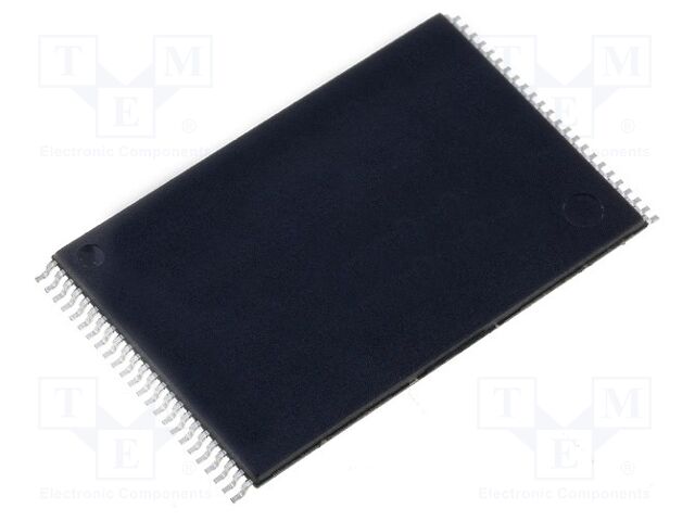
I would like to use Static RAM memory in external IC placed on PCB board connected with FPGA board. I would like to use 12-bit color for pixel displayed on HDMI monitor ( my FPGA board has HDMI interface). The minimu amout of memory needed for frame-buffer (HD) is 2Mega X 16-bit word. It is also important the type of case of selected SRAM IC in order to I be able to design PCB and solder memory chip to board. Currently I selected such SRAM IC:


It is SRAM chip organized as 2048K words by 16 bits. The single power supply is 1.65V-2.2V. Case is 48-Pin TSOP ,TYPE I ( 12mm x 20mm ) which I should be able to solder to printed circuit board. Here is data-sheet for this SRAM memory chip ( IS61/64WV204816ALL ):


I am not sure if I had selected optimal IC for this purpose - I mean the ease of writing driver in VHDL/Verilog for such SRAM memory. I am also not sure if driving such asynchronous SRAM in synchronic way from FPGA board would be working properly. If somebody can give me hints for such project i Will be very grateful.

Thanks in advance and regards
 

Asynchronous SRAM can be well interfaced with FPGA, you useally need multiple clock cycles per write or a multiphase clock to generate the write timing. Because asynchronous RAM is cheaper than synchronous RAM and better available, it's worth the effort.

What's the intended word rate in your application?
 

    FlyingDutch

    Points: 2
    Helpful Answer Positive Rating
Hello @FvM,

I think the word rate should be about 146 Mega words (word 16-bit) if i calculated it properly. The horizontal synchronization in HDMI is every 14.8 micro second. Assuming 1080 pixels in line - time for every pixel is 13.7 nanosecond: what gives frequency 72.97 MHz. This is only for displaying image, but I need dual port buffer (the same bit rate for writing to buffer from camera sensor). So the minimum frequency should be 145.95 Mhz.

Best regards
--- Updated ---

I think I aslo will need FIFO bufers on in and out from SRAM frame-buffer. I have also some questions how to implement dual port SRAM memory frame-buffer?
 
Last edited:

Hello @FvM,

I agree with you, I noticed that it is not feasible some time ago. I will try two things:

1) I reduce screen resolution to UXGA: 1600x1200
2) I will display screen with interlacing what should divide bitrate by two

I would like to use such camera sensor (OV2640):


The OV2640 camera sensor can send 15 frames per second with UXGA resolution (1600x1200 pixels). RGB565 color need 16-bit(two bytes) per pixel.
I calculated needed video bandwidth using this on-line calculator:


Bandwidth.png

For my camera OV2540 parameters calculated bandwidth is about 43.2 Mhz (without interlacing). With interlacing 21.6 Mega words (16 bit). But considering dual port interface to SRAM frame-buffer we finally has 43.2 Mega words (16-bit). it gives about 23.15 nanose3cond per operation on SRAM (writing/reading one wortd). Do you think @FvM it is feasible with such parameters to do it with IS61/64WV204816ALL IC ?

I would like also to ask how to design from hardware point of view such dual port interface to SRAM memory buffer? With using "Block Memory" from inside of FPGA it was very easy - I just use "Dual-port BlockMemory" IPCore from Xilinx. I am not sure how to design such dual-port memory interface from hardware and software point of view, so any comment would be very useful for me.

Best Regards


Hello,

I decided that first I will try to connect to FPGA board a smaller SRAM memory with organisation of memory: (256K x 16bit) Parallel 10ns in 44-TSOP case. I found in my drawer two SRAM memory ICs made by Cypress with symbol CY7C1041CV33-10ZSXI - here is link to it's data-sheet:

https://datasheet.octopart.com/CY7C1041DV33-10ZSXI-Cypress-Semiconductor-datasheet-17703221.pdf

This IC is obsolete now, but there are still active very similiar parts with symbol CY7C1041G10ZSXIT - they have the same pinout as CY7C1041CV33-10ZSX, and the same parameters. Here is link to it's page:

https://pl.mouser.com/ProductDetail/Cypress-Semiconductor/CY7C1041G-10ZSXIT?qs=/ha2pyFaduh0yemDg4h8iPRcd6uZg6jBuQMJjKFwlztWmTNJRjtfFg==

Frame-buffer made with CY7C1041CV33-10ZSXI SRAM would enable display video with resolution 640x480 16-bit color (with interlaced). I drewd a schematic for external PCB with this type of SRAM IC:

Schematic_CY7C1041_SRAM-Cpy_2020-10-17_17-58-53.pdf

In the next few days I will design a PCB and try to attach this memory buffer to FPGA board (of course this task also entail writing SRAM controler in HDL language). If I will have results I describe them here.

Best Regards
 

Attachments

  • Schematic_CY7C1041_SRAM-Cpy_2020-10-17_17-58-53.pdf
    94.3 KB · Views: 178

Hello,

this weekend I have some time to work a little on this subject. I modyfied a little a schematics: I added three jumpers in order to enable powering SRAM memory from not stabilized voltage from 5 to 8V given on two pins of socket (with use of internal 3.3 V stabilizer IC), or directly from stabilized 3.3 V from FPGA board. Here is modyfied schematics:
Schematic_CY7C1041_SRAM_2020-10-25_14-21-12.png


I also designed simple PCB board for SRAM memory IC and address , data and control busses connected to two rows socket in order to plug this board to FPGA.
--- Updated ---

Sorry I had to divide my post into two because of size - here is part two. Here is designed PCB board:


PCB_CY7C1041_SRAM_PCB1_2020-10-25_14-19-25.png


Could I ask for checking if this PCB is consisten with given schematics? I also attach to this post schematics and PCB project in PDF format and zipped sources for "EasyEDA" CAD (schematics and PCB).
 

Attachments

  • Schematic_CY7C1041_SRAM_2020-10-25_14-04-55.pdf
    101.9 KB · Views: 83
  • PCB_CY7C1041_SRAM_PCB1_2020-10-25_14-16-44.pdf
    80 KB · Views: 139
  • @CY7C1041_SRAM.zip
    44.9 KB · Views: 91
Last edited:

Hi,

I didn't check consistency. Can't this be done by the software?

My schematic recommendation:
* it usually makes not much sense to draw an IC symbol like it's physical dimension. Better is to combine pins according their function.
* use multiple GND and supply symbols instead of lenghty wires.

My PCB layout recommendations:
* Use bottom layer as GND plane.
* make all GND connections with very short traces and via to GND plane.
* place the ceramics capacitors as close as possible to the according IC pins.
* on the right side there are 11 blue lines crossing 3 red lines. Doing it the other way round (make the 3 vertical lines blue) saves at least 16 vias and keeps GND plane more solid.
* you may route wires underneath the SRAM IC on both layers.

Klaus
 

    FlyingDutch

    Points: 2
    Helpful Answer Positive Rating
Hello @KlausST,

thanks for helpful comments :) - especially one before last is very helpful for me. I will try to improve the PCB design in accordance with your comments.

Thanks and regards
 

Hello,

I improved the PCB - currently it contains less "via"s and has not DRC rules violation. I attached new PCB (pdf), gerber files and "EasyEDA" sources (zipped).


Best Regards
 

Attachments

  • PCB_CpyCYC71041SRAM_PCB3FIN_2020-10-27.pdf
    71.2 KB · Views: 110
  • Gerber_CpyCYC71041SRAM_PCB3FIN_2020-10-2.zip
    12.5 KB · Views: 77
  • SourcesEasyEDA.zip
    44.5 KB · Views: 76

Hello,

delivery from JCLPCB has just arrived and I have got PCB boards. Them looks nice - see photo:

IMG_20201105_155841.jpg


So I am going to connect this PCB board with SRAM CY7C1041CV33-10ZSXI to FPGA board with Artix-7 and try to run memory controller.

Best Regards
 

Hello,

today I have got PCB board mounted - see photo:

IMG_20201106_100810.jpg


Tomorrow I will try to launch this external board with CY7C1041CV33-10ZSXI SRAM IC and start writing memory controller in HDL (on FPGA board).

Best regards.
 

Status
Not open for further replies.

Part and Inventory Search

Welcome to EDABoard.com

Sponsor

Back
Top