Continue to Site

Welcome to EDAboard.com

Welcome to our site! EDAboard.com is an international Electronics Discussion Forum focused on EDA software, circuits, schematics, books, theory, papers, asic, pld, 8051, DSP, Network, RF, Analog Design, PCB, Service Manuals... and a whole lot more! To participate you need to register. Registration is free. Click here to register now.

Stablilize the cascade opamp

Status
Not open for further replies.

TuAtAu

Advanced Member level 4
Joined
May 22, 2011
Messages
119
Helped
9
Reputation
18
Reaction score
9
Trophy points
1,298
Location
Jupiital
Activity points
2,149
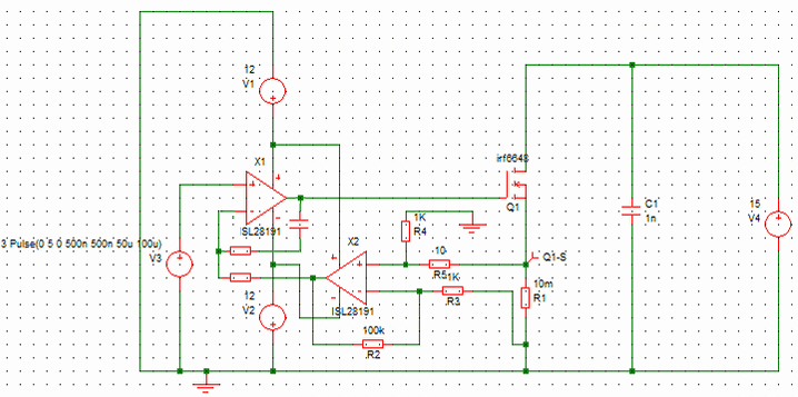
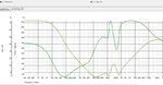
[Problem]Stablilize the cascade opamp

How to stabilize this cascade opamp. I had to amplify the sensing resistor to view in the oscilloscope for this current limiter.

How to prevent the oscillation~ any short note, advice or article?

:-?

problemre.png

**broken link removed**

**broken link removed**
sorry for inconvenience.. :oops:
 
Last edited:

Unfortunately, the left diagram tells us nothing and the right one is to small - that means, one cannot read resistor values (are there any?).
Please, concentrate on most important information.
 

After added feedback oscillator it started to oscillate. I don't want it.

First comment, you don't necessarily need to cascade amplifiers, because the shunt has the same ground reference as the input signal. But with sufficient fast OPs, you possibly get stability problems due to the MOSFET input capacitance even with a single OP.

If you sketch the loop gain magnitude and phase of your circuit (a bode diagram), you'll see, that it can't be stable with universal (unity gain) compensated OPs. Prefereably you would add an AC feedback path from X1 ouput to inverting input. Add a series resistor at X2 output and a RC series circuit for the feedback. Adjust the resistor ratio and time constant empirically or based on a calculation.

I need to have the amplifier to have 100 gain in order to view it in oscilloscope. As you know, the sensing Resistor has only 10mOhm, the voltage drop also in milliVolt. In oscilloscope it cannot show a smooth(distortion) graph.

The X1 is the comparator that compare with the pulse source to limit the current. If added feedback as unity, the current at MOSFET cannot follow exactly the same shape of the pulse source already.

Is it?
 

I thought about a compensation network like this:

49_1306942178.gif


P.S.: I see, that ISL28191 is a fast bipolar OP. You would want to use symmetrical resistor values in the differential amplifier to avoid additional offsets created by the the bias currents.
 

I thought about a compensation network like this:

49_1306942178.gif


P.S.: I see, that ISL28191 is a fast bipolar OP. You would want to use symmetrical resistor values in the differential amplifier to avoid additional offsets created by the the bias currents.

If do like that, the slew rate of the current at mosfet is differ with the power source at comparator. I wish the current follow the same shape of the power source at comparator non-inverting terminal terminal ...

But i try to adjust the R and C value.. still have a very high overshoot for the current at mosfet...
 
Last edited:

If do like that, the slew rate of the current at mosfet is differ with the power source at comparator. I wish the current follow the same shape of the power source at comparator non-inverting terminal terminal ...
First comment, X1 isn't working as a comparator. It's a linear amplifier in the current control loop. The loop gain magnitude and phase is determining the pulse response of the output current.

But i try to adjust the R and C value.. still have a very high overshoot for the current at mosfet...
Most likely you didn't yet find the optimal gain setting. In addition, you'll possibly observe difficulties to drive the MOSFET gate node capacitance with the OP output impedance. A small gate series resistance (10 - 20 ohm) may improve the setting range.

It's just elementary analog design.
 

even though I add a series resistance between the gate and the OP, Its still have the overshoot effect..

may I have more details on how to get ride of it?
**broken link removed**
 

Your mosfet is N-chan enhancement type. Its gate V is referenced to its source terminal (the more negative one).

You've got several components in contact with that terminal.

Some components carry signal back into the op amp which influences the op amp driving the mosfet.

Besides that, there's a resistor going to ground. This causes a certain amount of feedback effect at the mosfet gate.

I believe this is where your overshoots are coming from. A loop or two in your circuit needs to settle after the transition to high.

I don't know how to go about solving it, unless it's to use a P-channel mosfet instead. Its gate is referenced to the drain terminal (the more positive leg). However this would invert its operation.
 
Last edited:

Your mosfet is N-chan enhancement type. Its gate V is referenced to its source terminal (the more negative one).

You've got several components in contact with that terminal.

Some components carry signal back into the op amp which influences the op amp driving the mosfet.

Besides that, there's a resistor going to ground. This causes a certain amount of feedback effect at the mosfet gate.

I believe this is where your overshoots are coming from. A loop or two in your circuit needs to settle after the transition to high.

I don't know how to go about solving it, unless it's to use a P-channel mosfet instead. Its gate is referenced to the drain terminal (the more positive leg). However this would invert its operation.

Do you feel that PMOS or NMOS is better on this design? I m planning to draw about than 40A over the Rds(on) with certain duty cycle ofcause
 

In my opinion, there's no particular preference for a NMOS or PMOS in this circuit. You have to analyze the circuit's transmission function and dimension the compensation network for suffcient closed loop phase margin. Changing to PMOS will change the loop gain and loop gain sign and require respective circuit changes.
Some components carry signal back into the op amp which influences the op amp driving the mosfet.
Are you talking about the feedback loop?
Besides that, there's a resistor going to ground. This causes a certain amount of feedback effect at the mosfet gate.
Do you mean R1? What's the related "feedback" effect?

P.S.: I just realized, that the shown waveform (2V input 20 A output) apparently doesn't match the original circuit gain of 1A/V.
 
Last edited:

Resistor R1 is a feedback resistor in the same sense that a resistor creates feedback effect in the emitter leg of an NPN transistor.

When current (especially high current) goes through your mosfet, a voltage develops across R1. This has the effect of changing the relative voltage at the gate of the mosfet. (Because an N-chan mosfet has its gate V referenced to its source terminal.)

So let's see... The relative gate V is reduced.

This reduces current through the mosfet.

In turn this reduces the voltage across R1.

Raising the relative voltage at the mosfet gate.

This increases current through the mosfet. Etc. This process is a kind of feedback. It isn't the kind that leads to oscillations. Just a momentary ringing when the transition occurs.

Notice this feedback effect does not occur when the resistor is installed at the drain terminal of the N-mosfet (or at the collector of the NPN transistor).

In the simplest circuit this process occurs near the speed of light. It settles within a billionth of a second, maybe. And it's barely detectable.

So I don't know for sure that your overshoots are exclusively due to R1 being in the source leg.

But there's also your X2 op amp too. I don't know that X2 amplifies the slight ringing at R1. But it's situated where it could do so.

Or if not that, then it has its own tendency to overshoot. It adds a few propagation delays in the loop. Hence probably adding a bit of feedback of its own. Perhaps at the same frequency as R1. Or a different frequency.

I don't know exactly how to solve the overshoots. It seems to be the nature of the beast when you switch high currents.

It may help to put R1 at the drain leg of the mosfet instead of the source leg. You would have to revise your X2 operation.
 

Do you feel that PMOS or NMOS is better on this design? I m planning to draw about than 40A over the Rds(on) with certain duty cycle ofcause

From what I understand, N-mosfets usually perform better (faster), or have less 'ON' resistance, or are easier to operate, or are less expensive, etc.
 

Thanks for explaining your thoughts!
This increases current through the mosfet. Etc. This process is a kind of feedback. It isn't the kind that leads to oscillations. Just a momentary ringing when the transition occurs.
Notice this feedback effect does not occur when the resistor is installed at the drain terminal of the N-mosfet (or at the collector of the NPN transistor).
I agree, that R1 involves an internal feedback of the output stage (current controlled voltage feedback or "series-series" feedback). It's also true, that moving the current sense resistor to the transistor drain cancels this feedback. But why should this kind of feedback cause an overshoot?
 

Hi guys,
I try to upgrade the circuit but the overshoot problem still exist.

take a look.
**broken link removed**
 

Attachments

  • circuitpic.png
    circuitpic.png
    298.9 KB · Views: 69
  • freqx.png
    freqx.png
    284.3 KB · Views: 52
Last edited:

There is a flaw in my suggested compensation scheme in so far, that part of the setpoint signal is transmitted to the output directly. It should be modified by adding a R - RC network to the +ve input as well. The network can be adjusted to cancel the overshoot.

Connecting the compensation network to the MOSFET gate is not reasonable in my opinion.

Unfortunately, the circuit has a current dependent gain caused by the MOSFET transconductance variation. So you can't achieve a perfect pulse response for any output current.

that's mean there is no way to get a perfect square + slew rate? :cry:
 

I agree, that R1 involves an internal feedback of the output stage (current controlled voltage feedback or "series-series" feedback). It's also true, that moving the current sense resistor to the transistor drain cancels this feedback. But why should this kind of feedback cause an overshoot?

By itself a resistor in the emitter leg doesn't cause that much overshoot (looking at post #8). Anyway whatever voltage appears across the resistor, I imagine the mosfet gate is being driven by high enough voltage that the voltage across the resistor is immaterial.

So I think the overshoot is due to the feedback op amp. I don't know to what degree it might be exaggerating a ringing effect across the resistor, or whether the ringing comes from a delayed response effect around the loop, or within the loop, etc.
 

Status
Not open for further replies.

Similar threads

Part and Inventory Search

Welcome to EDABoard.com

Sponsor

Back
Top