Continue to Site

Welcome to EDAboard.com

Welcome to our site! EDAboard.com is an international Electronics Discussion Forum focused on EDA software, circuits, schematics, books, theory, papers, asic, pld, 8051, DSP, Network, RF, Analog Design, PCB, Service Manuals... and a whole lot more! To participate you need to register. Registration is free. Click here to register now.

SSTC (Solid State Tesla Coil) Halfbridge PCB Design

Status
Not open for further replies.

Alloy

Advanced Member level 4
Joined
Apr 3, 2016
Messages
116
Helped
0
Reputation
0
Reaction score
0
Trophy points
16
Activity points
1,003
Hello.
I am making a SSTC (Solid State Tesla Coil). That's a device which converts mains power (directly powered from 230V socket) to high voltage (100kV +).

The halfbridge is made of two IGBTs which are switched at around 200kHz (or less, I might go for 100kHz or so in the end).

I'd like to design my single-sided PCB well but I don't know where to start.

1. Can anyone recommend me any online readings, sites, videos, PDFs or ebooks related to high power/frequency PCB design?
2. Has anyone here designed a halfbridge single-sided PCB for Tesla or induction heater and can share his layout?

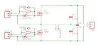
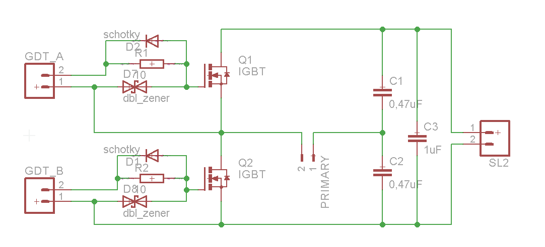
3. Please take a look at my halfbridge schematic and layouts:


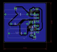
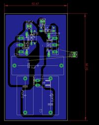
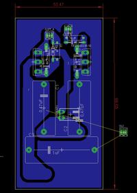
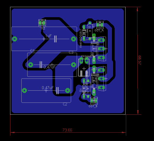
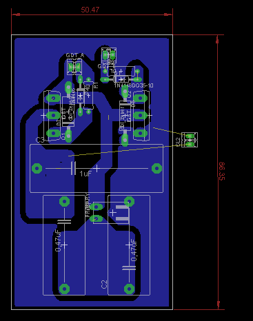
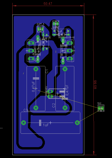
I have made three PCB layouts for this schematic:

LAYOUT A:

LAYOUT B:

LAYOUT C:


Which one of those PCBs is the best for so far and how can I improve it more? Any suggestions?

Thanks in advance.
 

i hope you are careful with that 100kv.........that can kill you even if you stand near it without touching it. Seriously kill you.
I once stood 50cm away from a 13kv terminal, my 4arm was 50cm from it, and i cold feel the muscle in my 4arm vibrating from the 13kv's electric field coupling up to me.

I think you may be gravely mistaken. You do not want to do this..surely
But regarding that bridge, it should use fets for that high frequency,
Also, you likely need a series dc blocking cap....or do it in current mode by putting a CST in there.
Otherwise those splitting caps will go asymetric

- - - Updated - - -

Also, add gate to source resistors, say 10k.
 
You are willing to risk your life just to make a big spark!!!

The full power of the 220v mains at 100KV will be there to electrocute you.
 
Last edited by a moderator:

The very high voltage isn't going to exist on the PCB, but rather in the coil itself. Still not an undertaking for amateurs.

I would start out by trying to imitate work by other experts such as Steve Ward and Rich Burnett.
 

Nobody said the high voltage was on the PCB, Treez talked about how the high voltage can jump and i tried to make it clear how much power would be available in that spark (but obviously not clear enough).

This thread is a good example of why didn't someone say something so this kid did not kill himself. Well i am saying something, AS STRONGLY AS I CAN.
 

I have already made several SSTCs (as well mains-powered) ones.

I know Stevie Wards and Richard Burnetts sites very well.

My question was related to the PCB design itself, how to avoid the stray inductances, improve the gate drive signal quality, and NOT about the HV itself.

My existing driver PCB has some ringing which is visible when I look at the osciloscope and that's something I wanted to fix.
 
Last edited by a moderator:

Good to hear that you apparently know about the risks of high voltage circuits. It's not really obvious when we read words like "I'd like to design my single-sided PCB well but I don't know where to start."

Consider that all responses are from experienced forum members who seriously care about your health.
 

If PCB design of switching power supplies is your interest here, then this document , on PCB layout of SMPS, will be of use..

- - - Updated - - -

Ringing in gate drives sounds like insufficient damping in the gate drive loop, or the loops involving the gate drive not being narrow-area enough so having stray inductance associated with them which rings with the stray capacitance.

- - - Updated - - -

Worth remembering that the "gate drive loop" isnt just the one obvious loop, -think of the loops involving through the CDS and where that goes off to thru' the primary etc.
(I remember a ex-workmate in Redditch once telling me he had tesla coils in his garage and he used to make stuff levitate with it...he said the high voltage used to ionise the air and the collection of ions floating about used to cause problems, so he told me he solved it by just putting a fan there and blowing the air ions away.)
 

Attachments

  • Basics of SMPS Layout _4.doc
    645.5 KB · Views: 105

First priority should be minimizing the inductance formed by the FETs/IGBTs and the bypass capacitor(s). But at the same time the FETs should be oriented such that they can be mounted to a good heatsink, which your layout doesn't seem to consider. Depending on your intended power level, you might consider using semiconductor modules instead of through-hole transistors. Also for frequencies above 100kHz, MOSFETs will usually outperform IGBTs.
 

Status
Not open for further replies.

Similar threads

Part and Inventory Search

Welcome to EDABoard.com

Sponsor

Back
Top