Continue to Site

Welcome to EDAboard.com

Welcome to our site! EDAboard.com is an international Electronics Discussion Forum focused on EDA software, circuits, schematics, books, theory, papers, asic, pld, 8051, DSP, Network, RF, Analog Design, PCB, Service Manuals... and a whole lot more! To participate you need to register. Registration is free. Click here to register now.

SRAM TIMING WAVEFORM

parminder

Member level 3
Joined
Mar 1, 2022
Messages
54
Helped
0
Reputation
0
Reaction score
0
Trophy points
6
Activity points
376
Hi,

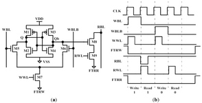
i have one query related to the SRAM timing diagram. can anyone please tell me where do we give the input of the clock that is shown in the reference image.

how do we decide when it is read cycle and when it is write cycle .

(Image for reference only).

thank you
 

Attachments

  • SRAM CLK.png
    SRAM CLK.png
    356.4 KB · Views: 223
  • Screenshot from 2023-05-18 11-42-03.png
    Screenshot from 2023-05-18 11-42-03.png
    387.1 KB · Views: 119
It looks like WBL and RBL and complementary signals and they decide when you are reading writing. But who knows, I don't know what this memory is supposed to do and where you got it from.
 
it is not about what wbl and RBL , my main concern is where CLK signal input is given , forget about 1st image. in second image also CLK signal is given. i have shared another image for reference.
 

Attachments

  • ab.png
    ab.png
    109 KB · Views: 104
A lone memory cell (a bit) theoretically needs no clock pulse. Thus it can be a simple RS flip-flop.

In practice memory cells are in groups of 8 bits, making a byte. It's necessary to keep all 8 actions synchronized (Read and Write). To perform these simultaneously, the 8 flip-flops are a kind which all obey the same clock pulse to the clock pin.
 
Last edited:
@BradtheRad well , being a beginner i have taken 16*8 array sram . for that i need clock and i am confused for this. and and i am using 6T sram array for that.
 
it is not about what wbl and RBL , my main concern is where CLK signal input is given , forget about 1st image. in second image also CLK signal is given. i have shared another image for reference.
can't you trace the clk and see where it arrives?
 
In my ancient experience with SRAMs the "clock" is generated by logic
from address transition detectors (along with any CE and R/Wb changes).

But DDRx SRAMs might have more "serial stuff" and the high speed
lines maybe do have an explicit clock. I have never had occasion to peel
back the lid on that.
 
SRAM doesn't use a clock. Imagine that the clock in the timing diagram is used to generate the control signals of the test setup.
 
Don't know what you specifically mean with write or read enable clock. I mean all control signals driving the circuit - all signals except for RBL which is an output generated by the RAM.
 
Alright , i am facing problem with multiple word line , Suppose i write data in 1 column 1 row after that write enable will be low and WL0 will also be low , now what is next. . If i want to read 1cl 1 row data, i have to make WL0 high . but how it will be done

i have attached an image for reference .
 

Attachments

  • transient response.png
    transient response.png
    157.3 KB · Views: 64
Last edited:
The read condition is RWLx = 1 and FTRRx = 0. You'll have decoders for binary row and column addresses to generate the signals.
 

LaTeX Commands Quick-Menu:

Part and Inventory Search

Welcome to EDABoard.com

Sponsor

Back
Top