Smillsey
Member level 5
Hi all
I have a general question about split power planes.
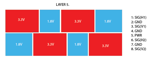
let’s look at an example of a split power plane on layer 5 of an 8 layer PCB.

There will be high speed signals on layer 3 and layer 6. Impedance calculations have been made for 100Ohm differential signal traces on layer 3, and other signal layers, the ground plane is closer (6mil) to the signal layers than this split power plane(15mil)
the power plane will provide power to ICs on the top and bottom layer, but these are power islands at the moment and I only have 1x 3.3V regulator and 1x 1.8V regulator to supply all islands
The 3.3v islands will become 1 plane.
can I simply daisy chain the 1.8V islands together, using vias to another layer and connecting with big traces through a via and running a thick trace to the next island?
or am missing something very obvious?
I have a general question about split power planes.
let’s look at an example of a split power plane on layer 5 of an 8 layer PCB.
There will be high speed signals on layer 3 and layer 6. Impedance calculations have been made for 100Ohm differential signal traces on layer 3, and other signal layers, the ground plane is closer (6mil) to the signal layers than this split power plane(15mil)
the power plane will provide power to ICs on the top and bottom layer, but these are power islands at the moment and I only have 1x 3.3V regulator and 1x 1.8V regulator to supply all islands
The 3.3v islands will become 1 plane.
can I simply daisy chain the 1.8V islands together, using vias to another layer and connecting with big traces through a via and running a thick trace to the next island?
or am missing something very obvious?
Last edited: