Welcome to our site! EDAboard.com is an international Electronics Discussion Forum focused on EDA software, circuits, schematics, books, theory, papers, asic, pld, 8051, DSP, Network, RF, Analog Design, PCB, Service Manuals... and a whole lot more! To participate you need to register. Registration is free. Click here to register now.
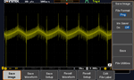
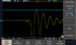
I designed cascaded converters and I have switching spikes at the output c6. spikes and zoom on each spike is attached. how to eliminate it? I used snubber circuit
Most of that noise is artifact from probing and other issues ( CM noise from the mosfet ) I can tell this because the volts go DOWN before they go up - as would normally be the case for a booster. In your case put a film foil cap from cathode to gnd on the boost diode ( short legs and ideally back to the fet source ) and then put a snubber on the boost diode ... ( you can also slow the turn on of the mosfet - this will help for RFI and your noise pickup on your scope probe )
Also add tight decoupling at the buck...eg a small ceramic value ceramic cap from buck fet drain to buck diode anode.
Also, of note is that you have no current sensing for either the boost fet or the buck fet...so it could be dangerous for you at eg startup or transient
It is soldered wires on board, I think the problem comes from mosfet paracitic capacitance. How to reduce it ? Should I increase the gate resistor or decrease it?
like written in your other thread. Every IC manufacturer and every MOSFET manufacturer provides application notes and design examples.
The are especially for unexperienced but also for experienced circuit designers. And they are for free. So use it.
They show you in detail what to care for and how to design the circuit and the PCB layout.
So you are doing an SMPS with stripboard and wires?....not a PCB.
My friend, i feel sorry for you....sorry but please stop now, you cannot do this. Its just too noisy.
Please see attached for PCB layout of SMPS...
This site uses cookies to help personalise content, tailor your experience and to keep you logged in if you register.
By continuing to use this site, you are consenting to our use of cookies.