Continue to Site

Welcome to EDAboard.com

Welcome to our site! EDAboard.com is an international Electronics Discussion Forum focused on EDA software, circuits, schematics, books, theory, papers, asic, pld, 8051, DSP, Network, RF, Analog Design, PCB, Service Manuals... and a whole lot more! To participate you need to register. Registration is free. Click here to register now.

SPI Timing Diagram

Status
Not open for further replies.

ku637

Advanced Member level 4
Joined
Apr 6, 2011
Messages
116
Helped
2
Reputation
4
Reaction score
3
Trophy points
1,298
Activity points
2,551
Hello,

This question may be not correct, but i would like to understand it better the SPI timing diagram. For CPOL=0 CPHA=0 I'm seeing in the following diagram <SPI Timing Diagram> that the MOSI and MISO first bits are shown as set even before the CLK started, right along with the SS signal going down.

Is it really like that i.e. an SPI master will place data (the first bit) on MOSI line even before the CLK started to appear and just when the CS is going down.


Thanks


[ADDED BY MOD]
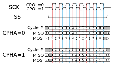
400px-SPI_timing_diagram2.svg.png
 
Last edited by a moderator:

Hi,

Please in future upload the according picture directly to edaboard. Since there is no guarantee that GOOGLE every time links to the same picture and there is no guarantee at all that the picture is not beeing deleted. .. and making the thread useless for the future.

****

I rather see this pictures as "example", it doesn´t scale timing.

For a more exact view you need to see the values for the timings.
So ther may be values from negative to zero, from zero to positive, or from negative to positive..depending on the setup and hold timing specification.

that the MOSI and MISO first bits are shown as set even before the CLK started, right along with the SS signal going down.
Usually MOSI and MISO timing is not related to the SS but the SCK signal.

usually SPI implementations use
* one SCK edge for OUTput of MOSI an MISO, means the value change close to this edge.
* and the other SCK edge is used to "clock in" the data to the receiving shift register. (IN edge)

-->
* there is no need to exactly output at the OUT edge,
* but there is the need for the data to be stable at the IN edge (including timing for setup and hold)

in your case the first clock edge is the IN edge ... but obviously before one can read IN data ... first the data needs to be sent out. Since there is no clock edge (in your case) it needs to relate to some other signal. The only chance is to relate it to CS.

With SPI all MISO signals need to be high impedance as long as CS = inactive ...
thus in your case CS is used to activate the OUTPUT driver to send out the first bit of data.

Klaus
 

    ku637

    Points: 2
    Helpful Answer Positive Rating
Status
Not open for further replies.

Similar threads

Part and Inventory Search

Welcome to EDABoard.com

Sponsor

Back
Top