Continue to Site

Welcome to EDAboard.com

Welcome to our site! EDAboard.com is an international Electronics Discussion Forum focused on EDA software, circuits, schematics, books, theory, papers, asic, pld, 8051, DSP, Network, RF, Analog Design, PCB, Service Manuals... and a whole lot more! To participate you need to register. Registration is free. Click here to register now.

SPI mode 0, data is transmitted at SCK falling edge, and ideally sampled at SCK rising edge. Will we design to have data sampled at SCK falling edge?

Status
Not open for further replies.

cczhangpjzj

Newbie level 4
Joined
Apr 21, 2008
Messages
7
Helped
0
Reputation
0
Reaction score
0
Trophy points
1,281
Activity points
1,353
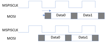
For SPI mode 0, functional operation is always data transmitted at SCK falling edge, then data is to be sampled at SCK rising edge.
But if you were to refer to https://www.ftdichip.com/Support/Documents/DataSheets/ICs/DS_FT800.pdf Figure 6-1 with Tod, the input to SPI slave is sampled at SCK rising edge. SPI slave output then seems it can be sampled at SCK falling or rising at the SPI master side.
And if you refer to https://datasheet.lcsc.com/lcsc/2101051104_Goodix-Technology-GR5515IGND_C2680494.pdf Figure 10-21 with tHMO/tHMO, this is similar that the data seems can be safely sampled at both SPIM SCK rising and falling edge.
Especially when SPIM SCK freq is high, then at SPIM side using SCK falling edge to sample input data can relax the setup time for SPIS output to SPIM input path. Is my understanding correct? And is people doing this way?
 

But if you were to refer to https://www.ftdichip.com/Support/Documents/DataSheets/ICs/DS_FT800.pdf Figure 6-1 with Tod, the input to SPI slave is sampled at SCK rising edge. SPI slave output then seems it can be sampled at SCK falling or rising at the SPI master side.
FT800 SPI interface sets MOSI at falling SCK edge. It will be regularly sampled at rising SCK edge. (Standard SPI mode 0 or 3), If the SPI bus involves longer round trip delay, sampling can be delayed to next falling edge, as supported by most SPI host interfaces.

You can check which method involves a larger sampling window margin. FT800 datasheet specifies minimal data hold time of 0 ns. If host samples MOSI data exactly at falling SCK edge, you have zero margin. Depending on the internal host timing, it could happen that MOSI is even sampled slightly after SCK edge, resulting in negative margin (data corruption) in this case. Thus you better use standard mode for slow and medium fast SPI interfaces.
Hi FvM, Thanks for your reply. I think I understand better overall. If now we talk about SPI master timing, and again for mode 0, the tVMO/tHMO defines the output delay from SCK falling edge to the output data MOSI for master SPI. I was not allowed to post the datasheet link this time. Basically this defines the output delay min/max range is 20~59ns which is the sampling window of SPI-slave. My question is that if I can delay SCK by like 35ns in SPIM, so that data change timing will be around SCK falling edge -15~14ns, this makes the relation of MOSI & SCLK at SPIM side more balanced. Then there should be better margin for SPI-slave to sample data at SCK rising edge. But I checked many SPIM timing info, it is always MOSI lagging behind SCK falling edge for both best and worst case. I never see any datasheet having MOSI could change earlier than SCK falling edge. Is there anything wrong with my thought.
Thanks!
 

Hi,

I don't see why you are not allowed to post a link.
instead of complicated and unprecise textual description, you could do a simple timing diagram draft to show your problem.

You give a couple of timings ... but surely no all to validate a communication.

What I miss is your intended SCK frequency.

If you need high speed SPI, then 20..59ns delay is rather unusual. Then I simply guess your device is not able to go the desired speed.

Klaus
 

Hi Klaus, sorry for the confusion. Earlier I copy a link, the thread got rejected. I copy the link here again, you need to go to the bottom. https://infocenter.nordicsemi.com/index.jsp?topic=/ps_nrf52840/spim.html
Yes 20~59ns delay is a bit too much. I use it just to illustrate the concept.

Below I make a waveform. Top is the typical timing waveform I see in many MSPI datasheet. There are 2 arrows, which defines the min/max output delay of MOSI from MSPISCLK falling edge.
Bottom is something that I suggest to have. Meaning MSPI side try to delay MSPISCLK internally in the chip.
This way, then the other side SPI slave could much better margin to sample it at rising edge of the SPI clock. I was just wondering why we don't do this way as in bottom. Thanks!

1674915494652.png
 

Attachments

  • 1674914713304.png
    1674914713304.png
    10.8 KB · Views: 84

Hi,
Basically this defines the output delay min/max range is 20~59ns which is the sampling window of SPI-slave.
I don´t see this. Where do you see this?

To me it´s still unclear how your SPI looks like, which IC is MASTER, which IC is SLAVE,
frequency... (already asked)
and a clear timing diagram which shows the problem (already asked)

...and why you want "sampled at falling edge at all" .. while you already know that mode0 does it at the rising edge.
One can do this only if both partners support this - but why?

Klaus
 

Hi Klaus, I think this thread starts with the question of spi-slave timing of its output (MISO), and then how host spi-master should sample the data MISO. This part is being discussed with FvM. That is host spi-master could use either SCK rising edge, or next SCK falling edge if the delay is too big.
I then asked the question of host spi-master timing of its output (MOSI). You may refer to myself drawn waveform with Tmax/Tmin as shown earlier. My question is shall we design spi-master timing of MOSI such that its changing time is centered around SCK falling, so that SPI-slave could sample it at SCK rising edge with more timing margin.

I think SPI mode 0 is SCK falling edge transmit the data & SPI rising edge to sample data. But in the real hardware IC design, because of long logic/PAD/PCB delay, we will optionally do a bit differently in order to have it support higher speed.

And earlier I have copied the link of some SPI master timing with 20/59ns output delay. Not sure why you did not see it. You may find it below with red highlighted. Its at the bottom of the webpage.
1674923148301.png
 

Hi,

I don't see that this 20/59 ns should be "in the sampling window".

Still missing important informations. I don't want to annoy you with repeated asking for them.
I'd better leave.

Klaus
 

Status
Not open for further replies.

Part and Inventory Search

Welcome to EDABoard.com

Sponsor

Back
Top