uglyduck
Junior Member level 2
Guys, I need some help with my circuit which I have attached below...
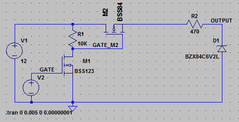
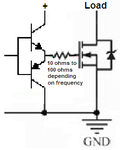
My circuit is intended to be a very cheap solution of a transmitter-receiver channel - the receiver is comprised of R1 and D1 and the rest components are the transmitter.
The problem is with the gate voltage of the p-channel mosfet. It seems to me that I cannot turn off fast the N-MOS in front of it. When there are only the N-MOS (BSS138 and not 123 as in the schematic) and the R1 resistor everything looks fine - sharp edges, no delays. But when I add the P-MOS then things go wrong - simulations attached.
10kHz
100kHz
[url=http://obrazki.elektroda.pl/6087576300_1398939803.png]
1Mhz
[url=http://obrazki.elektroda.pl/1883380800_1398939831.png]
I need to switch this circuit with up to 1MHz. As can be seen the N-MOS is ON very fast and than with the increase of the frequency it can be turned off much and much slower. At first I had doubts on the G-S capacitances, but BSS138 has ~25pF and BSS84 has ~45pF that is not as much. I tried to vary with that R1 value and also tried to pull down the N-MOS gate with resistors between 1k and 100k but no luck. What can I do about speeding up this circuit? Any ideas?
And one more question - is the output voltage (after the zener) always high because of the missing load - how can it be like that?
") Flipping the PMOS not solved the problem (that was a mistake in the simulation, but in the real circuit it's right - Drain is the output, Source is to the left). In simulation when flipped the result is the same. I have some success only if R1 is way too low - about 430 ohms. What is the explanation of that, what is the physical reason? Are there other solutions?
Flipping the PMOS not solved the problem (that was a mistake in the simulation, but in the real circuit it's right - Drain is the output, Source is to the left). In simulation when flipped the result is the same. I have some success only if R1 is way too low - about 430 ohms. What is the explanation of that, what is the physical reason? Are there other solutions?