Continue to Site

Welcome to EDAboard.com

Welcome to our site! EDAboard.com is an international Electronics Discussion Forum focused on EDA software, circuits, schematics, books, theory, papers, asic, pld, 8051, DSP, Network, RF, Analog Design, PCB, Service Manuals... and a whole lot more! To participate you need to register. Registration is free. Click here to register now.

Some questions about this class AB amplifier

Status
Not open for further replies.

boylesg

Advanced Member level 4
Joined
Jul 15, 2012
Messages
1,023
Helped
5
Reputation
10
Reaction score
6
Trophy points
1,318
Location
Epping, Victoria, Australia
Activity points
11,697
amplifier.jpg

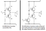
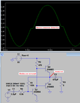
I assume R4 is the collector resistor for the class A common emitter (voltage gain) part of the amplifier (Q1).
And that R4 is in that position because it is the only place it can go with interfering with the class B part of the amplifier (Q2 & Q3)


However, class A common emitter amplifiers, by themselves, usually have an emitter resistor but they never seem to have one when they are part of a class AB amplifier. Why is that so?

And the other bit that I don't quit have my head around is the connection of R4 to the junction between Q2 and Q3 (through (C1). I understand that it is feedback, but why is it needed? What would happen if you connected R4 to Vcc, as is normally the case with a class A amplifier?
 

An emitter resistor is used for a transistor to provide DC and AC negative feedback to automatically adjust the base-emitter DC bias point and reduce AC gain and distortion.
Transistor Q1 already has DC and AC negative feedback through R6 so it doesn't need an emitter resistor.

The collector load impedance for Q1 is much higher than the value of R4 due to the "bootstrapping" provided to R4 by C1 and the speaker. Both ends of R4 have almost the same amount of signal level so the AC current in it is very low resulting in its impedance being very high. Bootstrapping by C1 causes the voltage at both ends of R4 to be able to swing above the +12V supply for higher signal levels and higher output power than if R4 was connected to +12V.
I looked in Google for Bootstrapping In Amplifiers and found many explanations like this one: **broken link removed**
 

An emitter resistor is used for a transistor to provide DC and AC negative feedback to automatically adjust the base-emitter DC bias point and reduce AC gain and distortion.

From what I have recently red about the subject, is this because an emitter resistor raises the emitter above ground a little and therefore reduces the voltage difference across BE and in turn reduces the current which in turn reduces the resulting CE current.

From that transistoramp software for designing class A amplfiers, the emitter resistor seems to always be a low value (well below 50R mostly).

Can I assume that if I mucked around with that transistoramp software I would eventually come up with a common emitter amplifier configuration that has a collector resistor but no emitter resistor. And that the voltage gain and input and output impedance that I selected
to produce such a configuration is roughly necessary when you connect a class A common emitter amplifier to a complementary pair arrangement?


How does Q1 drive both Q2 and Q3 exactly?

I can see how it probably drives Q3 - audio goes high, Q1 conducts, Q3's base voltage falls and Q3 therefore conducts?

I can intuitively see how Q1, Q2 and Q3 would drive the speaker if they were in this configuration:

**broken link removed**

But I am struggling to get my head around how they do so in the configuration I have actually used.
 
Last edited:

Nobody makes an amplifier like you show. If the driver transistor is an NPN then it can pull down the inputs of the output transistors and its collector load resistor pulls them up like this:
 

Attachments

  • amplifier.png
    amplifier.png
    30.8 KB · Views: 68

Bootstrapping by C1 causes the voltage at both ends of R4 to be able to swing above the +12V supply for higher signal levels and higher output power than if R4 was connected to +12V.
Well I did not know that was possible and I have never seen any page explain bootstrapping in the specific way you have described it here. It makes a lot more sense to me now.

I know that inductors can boost voltage above the supply level due to MC03463 and I suppose the speaker is effectively an inductor.

But capacitors on their own can't boost voltage above supply level can they?

What would happen to the sound if I removed the negative feed back?
 

The inductance of the speaker is not causing the output voltage boosting with bootstrapping. The output capacitor (or bootstrap capacitor in a circuit where the speaker connects to ground and has its own output capacitor) does the bootstrapping because the capacitor always has the same DC voltage across it. when the lower end of the capacitor is driven positive by the signal then its upper end also goes positive and goes above the supply voltage when the levels are high.

Here is a comparison between using the speaker and using a resistor to do the bootstrapping. Using the output capacitor and speaker to do the bootstrapping causes the driver transistor to flow in the speaker which is not good. Using an additional resistor and capacitor to do the bootstrapping is used in excellent amplifiers.

Here is another comparison of a bootstrapped amplifier and the same amplifier without bootstrapping. The gain is much lower without bootstrapping so the input level was almost doubled so the output level was almost as high as with bootsrapping. The distortion without bootstrapping is horrible.

- - - Updated - - -

What would happen to the sound if I removed the negative feed back?
Without negative feedback then the transistor might be DC saturated or DC cutoff depending on the temperature and selection (even transistors with the same part number) of the transistor.
The gain will be too high and the distortion will be horrible.

You can calculate or simulate the DC conditions yourself but I simulated the AC conditions here using the same transistor after carefully adjusting its bias voltage and reducing the input level:
 

Attachments

  • bootstrapped power amp.PNG
    bootstrapped power amp.PNG
    62.5 KB · Views: 109
  • bootstrapping.PNG
    bootstrapping.PNG
    43.5 KB · Views: 71
  • negative feedback.png
    negative feedback.png
    50 KB · Views: 69

The inductance of the speaker is not causing the output voltage boosting with bootstrapping. The output capacitor (or bootstrap capacitor in a circuit where the speaker connects to ground and has its own output capacitor) does the bootstrapping because the capacitor always has the same DC voltage across it. when the lower end of the capacitor is driven positive by the signal then its upper end also goes positive and goes above the supply voltage when the levels are high.

Here is a comparison between using the speaker and using a resistor to do the bootstrapping. Using the output capacitor and speaker to do the bootstrapping causes the driver transistor to flow in the speaker which is not good. Using an additional resistor and capacitor to do the bootstrapping is used in excellent amplifiers.

Here is another comparison of a bootstrapped amplifier and the same amplifier without bootstrapping. The gain is much lower without bootstrapping so the input level was almost doubled so the output level was almost as high as with bootsrapping. The distortion without bootstrapping is horrible.
So bootstrapping is to keep the currents through Q1 minimal and in the optimal range - I understand how clipping distortion happens in a class A amplifiers.

With this amplifier configuration.....

When the audio signal swings high, Q1 starts conducting and the base Q3 (PNP) goes low and it starts conducting current through the speaker and C1 to groud.
Which means that the voltage across R6 must drop a bit, Q1 conducts a bit less along with Q3. So this is clearly negative feedback that prevents a runaway process.


When the audio signal swings low, Q1 does not conduct and the base of Q3 remains high and it also does not conduct any current from the speaker through C1 to ground.

And here is my mental block.

What is responsible for turning on Q2 because the collector of Q1 is blocked by the diodes in this configuration.

Perhaps I need to set this circuit up in that javascript animation thing so I can see what is going on.
 

So bootstrapping is to keep the currents through Q1 minimal and in the optimal range
No. The value of R1 sets the correct amount of current in Q1. DC negative feedback adjusts the current for transistors having different Vbe and different amount of current gain.

I understand how clipping distortion happens in a class A amplifiers.
Clipping occurs when the input signal level is too high and causes the output signal level to try to swing above the supply voltage or below ground which are impossible.

When the input signal swings high, Q1 starts conducting and the base Q3 (PNP) goes low and it starts conducting current through the speaker and C1 to ground.
Which means that the voltage across R6 must drop a bit, Q1 conducts a bit less along with Q3. So this is clearly negative feedback that prevents a runaway process.
Negative feedback simply cancels some of the input signal to reduce the gain and reduce the distortion.

When the audio signal swings low, Q1 does not conduct and the base of Q3 remains high and it also does not conduct any current from the speaker through C1 to ground.
No. Q1 never turns off. It simply conducts a little more then conducts a little less. The same with the output transistors.

What is responsible for turning on Q2 because the collector of Q1 is blocked by the diodes in this configuration.
The resistors above the diodes turn on Q2 a little more when Q1 conducts a little less. The diodes add some base bias voltage to the output transistors so they never turn off. Severe crossover distortion will be caused if the diodes are replaced with a piece of wire like this:
 

Attachments

  • crossover distortion.png
    crossover distortion.png
    21.2 KB · Views: 121

Audioguru, I really appreciate your patience with me over this circuit.

I have implemented this circuit, plugged it into my PC headphone socket, plugged my speakers into the outlet of my amplifier and it works beautifully.

But that is not enough for me - I need to fully understand the circuit, at least to a reasonable level.

I will tell you the bits about this circuit that I do have a pretty good understanding of.

I understand that the class A bit is biased in such a way that it is continually conducting (CE) at a level roughly halfway between saturation and cutoff. When a positive audio signal goes into the base it (CE) conducts closer to saturation and when a negative audio signal goes into the base it conducts at a lower level closer to cutoff. If the audio signal amplitude goes too high or to low then the CE output will become clipped as the transistor enters saturation or cutoff.

With the complementary pair bit, I understand that they are both biased by the diodes at just above cutoff so that they are both on hair triggers and will start conducting with the least little input signal. If not then about +-0.7V of the input signal would be lost in biasing those two transistors before they start amplifying the input signal. And that this is cross over distortion. I further understand that the NPN exclusively amplifiers the positive parts of the audio signal and the PNP exclusively amplifies the negative part of the audio signal.

But I do not have an integrated understanding of this circuit, i.e. how these two components interact with each other in this configuration.

Can you try explaining it to me piece by piece?
When the amplifier is processing the positive part of the audio signal and assuming that there is a speaker between C1 anode and Vcc.

As I understand it the input signal plus bias current flows through Q1 base to ground and therefore Q2 is turned on via a current flowing along the path Vcc => speaker=> R4 => D1 => D2 => Q1 C => Q1 E => GND

Q2 therefore conducts a larger current along the path Vcc => Q2 C => Q2 E => R2 => C1 cathode
But then where does it go? The only path is back to Vcc across C1 and this is one bit I just can't get my head around.

In most amplifier schematics I have looked at it would flow to GND but that can't happen in this case.


If Q1 is conducting then the voltage at the base of Q3 must drop and it must start conducting?

Another thing that must be contributing to my confusion is that amplifiers often have a split supply so that the C of Q3 would normally be connected to -12V rather than GND, which would require a different configuration.

- - - Updated - - -

Ignore the previous post please as I ran out of time to edit it.

Audioguru, I really appreciate your patience with me over this circuit.

I have implemented this circuit, plugged it into my PC headphone socket, plugged my speakers into the outlet of my amplifier and it works beautifully.

But that is not enough for me - I need to fully understand the circuit, at least to a reasonable level.

I will tell you the bits about this circuit that I do have a pretty good understanding of.

I understand that the class A bit is biased in such a way that it is continually conducting (CE) at a level roughly halfway between saturation and cutoff. When a positive audio signal goes into the base it (CE) conducts closer to saturation and when a negative audio signal goes into the base it conducts at a lower level closer to cutoff. If the audio signal amplitude goes too high or to low then the CE output will become clipped as the transistor enters saturation or cutoff.

With the complementary pair bit, I understand that they are both biased by the diodes at just above cutoff so that they are both on hair triggers and will start conducting with the least little input signal. If not then about +-0.7V of the input signal would be lost in biasing those two transistors before they start amplifying the input signal. And that this is cross over distortion. I further understand that the NPN exclusively amplifiers the positive parts of the audio signal and the PNP exclusively amplifies the negative part of the audio signal.

But I do not have an integrated understanding of this circuit, i.e. how these two components interact with each other in this configuration.

Can you try explaining it to me piece by piece?
When the amplifier is processing the positive part of the audio signal and assuming that there is a speaker between C1 anode and Vcc.

As I understand it the input signal plus bias current flows through Q1 base to ground and therefore Q2 is turned on via a current flowing along the path Vcc => speaker=> R4 => Q2 B => Q2 E => R2 => C1 cathode => ????

Q2 therefore conducts a larger current along the path Vcc => Q2 C => Q2 E => R2 => C1 cathode => ????

But then where do these currents flow? The only path is back to Vcc across C1 and this is one bit I just can't get my head around.

In most amplifier schematics I have looked at it would flow to GND but that can't happen in this case.


If Q1 is conducting then the voltage at the base of Q3 must drop and it must start conducting?
 
Last edited:

I understand that the class A bit is biased in such a way that it is continually conducting (CE) at a level roughly halfway between saturation and cutoff. When a positive audio signal goes into the base it (CE) conducts closer to saturation and when a negative audio signal goes into the base it conducts at a lower level closer to cutoff. If the audio signal amplitude goes too high or to low then the CE output will become clipped as the transistor enters saturation or cutoff.
Yes.

With the complementary pair bit, I understand that they are both biased by the diodes at just above cutoff so that they are both on hair triggers and will start conducting with the least little input signal. If not then about +-0.7V of the input signal would be lost in biasing those two transistors before they start amplifying the input signal. And that this is cross over distortion. I further understand that the NPN exclusively amplifiers the positive parts of the audio signal and the PNP exclusively amplifies the negative part of the audio signal.
The output transistors are emitter-followers with plenty of current gain but no voltage gain. The first CE transistor has a fairly low amount of output current that can drive the bases of the emitter-followers then the high output currents of the emitter-followers drive the speaker and the bootstrapping.
The output capacitor has a continuous DC voltage of about half the supply voltage across it which is very important in this circuit with a single positive supply. Then since the top wire of the speaker is connected to +9V, the bottom wire of the speaker swings from about +5V to about +13V. When there is no signal then both wires of the speaker are at +9V.

When the amplifier is processing the positive part of the audio signal and assuming that there is a speaker between C1 anode and Vcc.

As I understand it the input signal plus bias current flows through Q1 base to ground and therefore Q2 is turned on via a current flowing along the path Vcc => speaker=> R4 => D1 => D2 => Q1 C => Q1 E => GND

Q2 therefore conducts a larger current along the path Vcc => Q2 C => Q2 E => R2 => C1 cathode
But then where does it go? The only path is back to Vcc across C1 and this is one bit I just can't get my head around.
Q1 is always conducting caused by it being biased by R1. The input signal causes it to conduct a little more and conduct a little less.
R2 provides base current for turning on Q2.
Q2 conducts more when Q1 conducts less, and Q2 conducts less when Q1 conducts more.

Q1 collector current turns on the base of Q3.
Q3 conducts more when Q1 conducts more, and Q3 conducts less when Q1 conducts less.

If Q1 is conducting then the voltage at the base of Q3 must drop and it must start conducting?
Without an input signal then Q1 is conducting enough so that its collector voltage can swing up and down. Q2 and Q3 are conducting a little to prevent crossover distortion.
If the input signal goes a little positive then it turns on Q1 more which turns on Q3 more. Then the emitter voltage of Q3 drops.
 

Status
Not open for further replies.

Part and Inventory Search

Welcome to EDABoard.com

Sponsor

Back
Top