Continue to Site

Welcome to EDAboard.com

Welcome to our site! EDAboard.com is an international Electronics Discussion Forum focused on EDA software, circuits, schematics, books, theory, papers, asic, pld, 8051, DSP, Network, RF, Analog Design, PCB, Service Manuals... and a whole lot more! To participate you need to register. Registration is free. Click here to register now.

Snubber required for VFD

Status
Not open for further replies.

adnan012

Advanced Member level 1
Joined
Oct 6, 2006
Messages
468
Helped
2
Reputation
4
Reaction score
2
Trophy points
1,298
Activity points
4,923
hi,

I am working on VFD to control the speed of a 5HP 3 phase induction motor using V\F technique. I need help in designing RC snubbers.

DC bus is 400V.
IGBT used is IRG4PC50W
Switching frequency 20KHz.
 

It's very unsual to have RC snubbers in IGBT or MOSFET based inverters.
 
There are many high power IGBT Half-Hridge Modules which have built in Snubber. I saw such a module in an old 30hp VFD.
 

You are talking about RC snubbers, not bus capacitors which are also sometimes designated snubbers?

I don't see RC snubbers in any recent inverter design.
 
Thanks for reply.

Can you explain why RC snubbers are not used in VFD?

How many DC bus capacitors are required for 5HP 440 v 3pahse inverter?

Do i need to add line reactors on the motor side?
 

You should not need to use RC snubbers in a VFD motor drive. You will need to pay particular attention to the loop inductance between the DC link capacitors and the IGBT DC terminals, as when the current is interrupted, the overshoot voltage across the IGBT becomes V = L.(di/dt), where L is the parasitic inductance, and the rate of change of current. In the interst of controlling switching losses, you need di/dt to be fast, so L has to be as small as possible. What normally happens is that the DC terminals of the IGBT have a very low SER polyester capacitor to soak up the voltage overshoot. This gives a clue on how to size it in order to control this voltage.

The number of DC bus capacitors is dictated by how much ripple your capacitors can stand, not only from the rectifier (if that's what you're using) but also the circultaing current from the inverter, and morelarticularly the magnetizing current for the motor interacting with the inverter and DC link cans.

You should not need line reactors on the motor side if you are using an inverter rated motor.

Finally be careful of shoot through and make sure you have enough deadtime. You can determine if you have enough deadtime by running you inverter with no motor at zero fundamental frequency. If you are drawing power and heating your devices, then you are shooting through.
 
If you have a semiconductor module with large IGBTs, along with a local DC bus capacitor (which is often referred to as a "snubber") then the parasitic inductance in that loop should be pretty low. Additionally, IGBTs do not switch very fast, so RC snubbers shouldn't be necessary. If you were using discrete semiconductors with poor layout, or some very fast devices like SiC FETs, then they might be necessary.
 
Actually the DC us capacitors are not considered snubbers. You really ought to have separate low inductance and low ESR capacitors closely mounted to the DC terminals of the IGBT module package, or across the common DC terminals of your discreets (or even one per upper and lower pair).

Yes the inductance should be pretty low, but when the inverter is in trouble and it is suffering a spanner on it's output then any whiff of inductance can be a major problem, particularly with a very low impedance fault, where the fault current could reach kA's. When you finally turn off the device in this state, the voltage spike can be enough to pop the IGBT. If this happens then all bets are off and you are then relying on fuses on the AC side.

Poor layout is your worst enemy. When I design an inverter, I purposely cause a shoot through with a large bank of caps attached to make sure it will survive a 10us shoot through, with regards to overshoot volts. That then proves your gate drive is stable under the worst of conditions, and your layout is sound.

Cheers,

Rob.
 
hi,

I am very thankful for your reply. I want to ask the following question.

1)What is the proper layout for such type of inverter? (gate driver to IGBT , Motor connection to Inverter connection etc).

2)Is it necessary to to use 3phase inverter module instead of discrete IGB's?

3)In case of discrete IGBT's (with internal fly wheeling diode) , do i need to add extra high power external anti parallel diode?

4) I am currently following
Microchip Application note AN843
"Speed Control of 3-Phase Induction Motor Using PIC18 Micro controllers"

It is designed for low power motors. Can i use it for high power motors by using high power Switching devices and current sensing components (hall effect sensor)?

5) do i need to have isolated power supplies to driver the switching devices, instead of using gate driver such as IR2109 (built in dead time)?

6) If the power source is only DC (Solar Panels), then in this case , do i need less number of DC buss capacitors?

7) What will happen if i have a submersible pump with 100-300 feet cables?

Regards
 

Actually the DC us capacitors are not considered snubbers. You really ought to have separate low inductance and low ESR capacitors closely mounted to the DC terminals of the IGBT module package, or across the common DC terminals of your discreets (or even one per upper and lower pair).
Right, this is what I meant above when I said "local DC bus capacitors." Usually a metalized polypropylene cap on each half bridge.
 
Hello,
1, Your layout for the gate drive should be as tight as possible while still maintaining creepage and clearance. You are driving the gates of the IGBTs, which are essentially capacitors. Any inductance and it will oscillate (with a poor Q because of the gate resistor). Output to the motor does not really matter too much as long as there is enough copper for the current.

2, It is easier to use an IGBT module, as someone has already optimised the layout int he module, you just need the external snubbers/decoupling cap(s).

3, No you should not need extra diodes.

4, You should be able to use this device with higher power motors as long as the feedback is scales correctly.

5, It is better to control and set up your own dead time, particularly with bigger devices, Normally the process PWM block has this as a function register.

6, You will still need extra capacitors if your supply is DC for the sake of control stability, have a google for middlebrook.

7, If you are on long cables, then the cable charging currents can affect your inverter, and can cause current trips. Have a look at this: **broken link removed**

Hope that helps.

Regards,

Rob.

- - - Updated - - -

Hi,
Yes mtwieg you are right, just misunderstanding..

To answer adnda012....

1, You are driving an IGBT who's gate is essentially a capacitor. Therefore any inductance in that loop can cause oscillation, and poor drive. You need to keep that loop as tight as possible while still satisfying creepage and clearance.

2, I tend to use modules as they are tidier, and tend to make thing easier from when you come to run the circuit, ie, less to go wrong.

3, No you won't need an extra diode.

4, Yes you can drive higher power motors as long as you scale you feedback as you say.

5, Much better to set your own dead time through your PIC on board PWM module. There should be a deadtime register. Use that. Excessive dead time affects 5th and 7th harmonic and increases machine losses.

6, I would still have plenty of DC capacitors; google middlebrook instability.

7, There are effects of driving long cables which may cause current trips. This is to do with cable capacitance and its critical impedance.

Have a look at: http://www05.abb.com/global/scot/scot239.nsf/veritydisplay/fec1a7b62d273351c12571b60056a0fd/$file/voltstress.pdf

Hope that helps.

Regards,

Rob.
 
Expect an extended learning curve when starting power electronics design. It's unlikely that your first attempt will succeed, starting a higher power inverter design from the scratch is big project. Unless you're required to do it (e.g. because you have been fearless enough to chose it as a finals year poject) consider buying a cheap chinese inverter. You'll hardly cope with the costs anyway.
 
Agree with FvM, and don't kill yourself. Drives can be lethal, particularly with ref to stored charges. Is this a Uni project? It's a bit ambitious for a final year project but I wish you lots of luck.

Regards,

Rob.
 
Expect an extended learning curve when starting power electronics design. It's unlikely that your first attempt will succeed, starting a higher power inverter design from the scratch is big project. Unless you're required to do it (e.g. because you have been fearless enough to chose it as a finals year poject) consider buying a cheap chinese inverter. You'll hardly cope with the costs anyway.

My learning curve (the past 18 months) in power electronics has been very steep and expensive. It is paying off, but only after some very unexpected and long lessons. The project being discussed is not an easy one as others have pointed out.

PCB layout for this type of circuit is sort of a black art, no book, video, or forum can tell you how to lay out your board. You have to develop a feel for the current loops and the parasitic inductance your design will create. You won't really know what you have until you have spun the PCB, built it and tested it. Snubbers can be used to cover mistakes but they dissipate heat. the better the PCB layout, the less likely you will need any snubber or at least it can be a gentle one.

Testing and observing these circuits can be quite a challenge as well. First off, it's dangerous to your life if you make a mistake. Second, measurement technique is critical of you will end up chasing your tail if you are not measuring correctly. I spent a considerable amount of time trying to shape an overshooting gate pulse that was on my scope. As it turned out, the gate pulse was fine, and I was using a long gnd lead on my probe. Also, you will need a scope many orders of magnitude faster than your switching frequency to see the overshoots and ringing that your snubbers will be attenuating. I would consider putting in dedicated test points that have a GND via very close to points of interest - gates, switch nodes, etc. They make it much easier to test properly and reduce the possibility of damaging yourself, your scope, or your circuit.
 
rule of layout = 1...keep high frequency power switching currentloops as narrow in area as possible.
2....Don't route high dv/dt traces too near high impedance inputs
3....Don't route high di/dt power current pulses through your controlle ground.
4.....Route input power traces as diff pair (go and return together)
5.....Remember the gate drive loop is high di/dt too.
6.....using series gate resistance, delay the drain voltage transition of the igbt to make switching less noisy.

That's a good bit of the rules of layout.
We had a consultancy tell us that layout was magic and only they could do it.....as long as we payed them 10's of thousands.

These rules will save you a few revisions and quite a few hours of troubleshooting. Excellent summary of the typical issues.

My primary encouragement to learn power electronics was that other engineers and layout people tried their best to convince me it was magic as well. What I learned is that it is not magic, but it is also not always obvious when it comes down to laying out your own design. Many times, it is hard to tell the difference between a schematic or component issue and a layout issue. Eventually, I learned the analysis and troubleshooting needed to find the problems quickly. The ultimate goal is to do it once, but that does not seem to happen even for engineers with far more experience I do.
 
This helps answer the original question about RC snubbers and that the DC link capacitor is doing the job of snubbing.

https://answers.yahoo.com/question/index?qid=20101112135332AAEPsBD

A DC link exists between a rectifier and an inverter, for example, in a VFD or phase converter. On one end, the utility connection is rectified into a high voltage DC. On the other end, that DC is switched to generate a new AC power waveform. It's a link because it connects the input and output stages.

The term "DC link" is also used to describe the decoupling capacitor in the DC link. I assume that this is what you're asking about. The switching network on the output side generates very large transients at the switching frequency. The DC link capacitor helps to keep these transients from radiating back to the input. This can also help prevent the switching network from oscillating or triggering inadvertently at an inappropriate moment and causing a short. Additionally, if the input is not multiple-phase, the capacitor helps provide a source of energy when the input waveform is near zero.
 
I am thankful for all of you for helpful comments.

For safety reasons, initially i will drive the devices at low voltage and power levels.

I have selected IRG4PC50UD IGBT (after successful testing i will get IGBT 3 PHASE Module ). Currently i am building a half bridge to drive a dc motor.

Regards

- - - Updated - - -

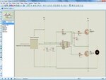
I am working on a half_Bridge as shown in the attached file.

20KHZ PWM is generated by PIC18F4550. PWM signal is fed to Opto coupler FOD3120.
Micro controller and FOD3120 input side have separate ground.

FOD3120 output side is connected to the IR2109 (gate driver). Opto coupler (output side) , Gate Driver and IGBT have same ground.

Micro-controller is programmed to generates PWM (20KHz) with a duty of 10%. After every second duty cycle is incremented with a 5% step and reaches to 90% duty. The motor works fine during this period. it draws 1 amp current under no load conditions.

On oscilloscope i can verify the gate signals on both igbt' gates. 14 -15 volt at the gate of the lower IGBT and (28+ 15- vf) = 42 volts with respect to system ground. These Gate voltage are valid for all Duty cycles.

But when the micro-controller starts decreasing duty cycle in the same manner (90% to 10% with 5% decrement after every second) the gate voltage at the high side igbt fluctuates. And the gate drive ic is damaged. However IGBTs, opto-coupler and controller are safe

So far i have burned 2 driver ic. I need help to sort out the issue.

IR2109 output current limit is 120 mA / 250 mA. What is the peak gate current required to drive IGBT ?
 

Attachments

  • HalfBridge_Motor_Driver.JPG
    HalfBridge_Motor_Driver.JPG
    70.2 KB · Views: 174
  • FOD3120.pdf
    407.5 KB · Views: 85
  • ir2109.pdf
    350.3 KB · Views: 86
  • irg4pc50ud.pdf
    219.5 KB · Views: 74
  • mbrd320.pdf
    182.9 KB · Views: 75

Status
Not open for further replies.

Similar threads

Part and Inventory Search

Welcome to EDABoard.com

Sponsor

Back
Top