Smillsey
Member level 5
Hi all
I hope you can help, I have been trying to get my head around gain/phase margins in LT spice and I have been following an Intersil App note (https://www.intersil.com/content/dam/Intersil/documents/tb41/tb417.pdf)
I have been able to design and simulate the output filter stage correctly and I achieve the same bode plots as expected when comparing to the app note and my own mathematics. (The double pole and ESR zero behaves as expected, dipping down near to -180deg and then the ESR zero pulls the phase back around closer to -90deg)
Yet when I come to design the compensator (Type 3) I am getting really confused with the phase response of the system, specifically the compensator phase behaviour.
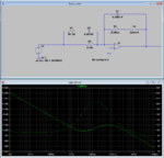
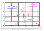
I tried to create the compensator on its own in LT spice and ran a bode plot on it, I am just using an ideal op amp model for now. This gives the expected zero's and pole's for the gain but I am mystified why I cannot get the same "-90deg to +90deg then to -90deg" phase response as shown in the Intersil app note.
Instead, my bode plots for the compensator start at 90, rise to around 210 and fall off. The overall shape is correct but I am not "starting" at the correct phase.
I have attached an image of the simple circuit, I have arrange the circuit as an inverting op amp as required.

I am pulling my hair out with it, have I misunderstood the phase response of this circuit?
Why doesn't it resemble the phase response in the image below?

Any help will be greatly appreciated.
Feeling pretty dumb right now :thumbsup:
I hope you can help, I have been trying to get my head around gain/phase margins in LT spice and I have been following an Intersil App note (https://www.intersil.com/content/dam/Intersil/documents/tb41/tb417.pdf)
I have been able to design and simulate the output filter stage correctly and I achieve the same bode plots as expected when comparing to the app note and my own mathematics. (The double pole and ESR zero behaves as expected, dipping down near to -180deg and then the ESR zero pulls the phase back around closer to -90deg)
Yet when I come to design the compensator (Type 3) I am getting really confused with the phase response of the system, specifically the compensator phase behaviour.
I tried to create the compensator on its own in LT spice and ran a bode plot on it, I am just using an ideal op amp model for now. This gives the expected zero's and pole's for the gain but I am mystified why I cannot get the same "-90deg to +90deg then to -90deg" phase response as shown in the Intersil app note.
Instead, my bode plots for the compensator start at 90, rise to around 210 and fall off. The overall shape is correct but I am not "starting" at the correct phase.
I have attached an image of the simple circuit, I have arrange the circuit as an inverting op amp as required.

I am pulling my hair out with it, have I misunderstood the phase response of this circuit?
Why doesn't it resemble the phase response in the image below?

Any help will be greatly appreciated.
Feeling pretty dumb right now :thumbsup: