Continue to Site

Welcome to EDAboard.com

Welcome to our site! EDAboard.com is an international Electronics Discussion Forum focused on EDA software, circuits, schematics, books, theory, papers, asic, pld, 8051, DSP, Network, RF, Analog Design, PCB, Service Manuals... and a whole lot more! To participate you need to register. Registration is free. Click here to register now.

SMPS design problems

Status
Not open for further replies.

Hz2020

Member level 3
Joined
Nov 11, 2011
Messages
57
Helped
11
Reputation
22
Reaction score
11
Trophy points
1,298
Activity points
1,637
Hello Guys,

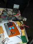
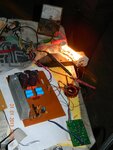
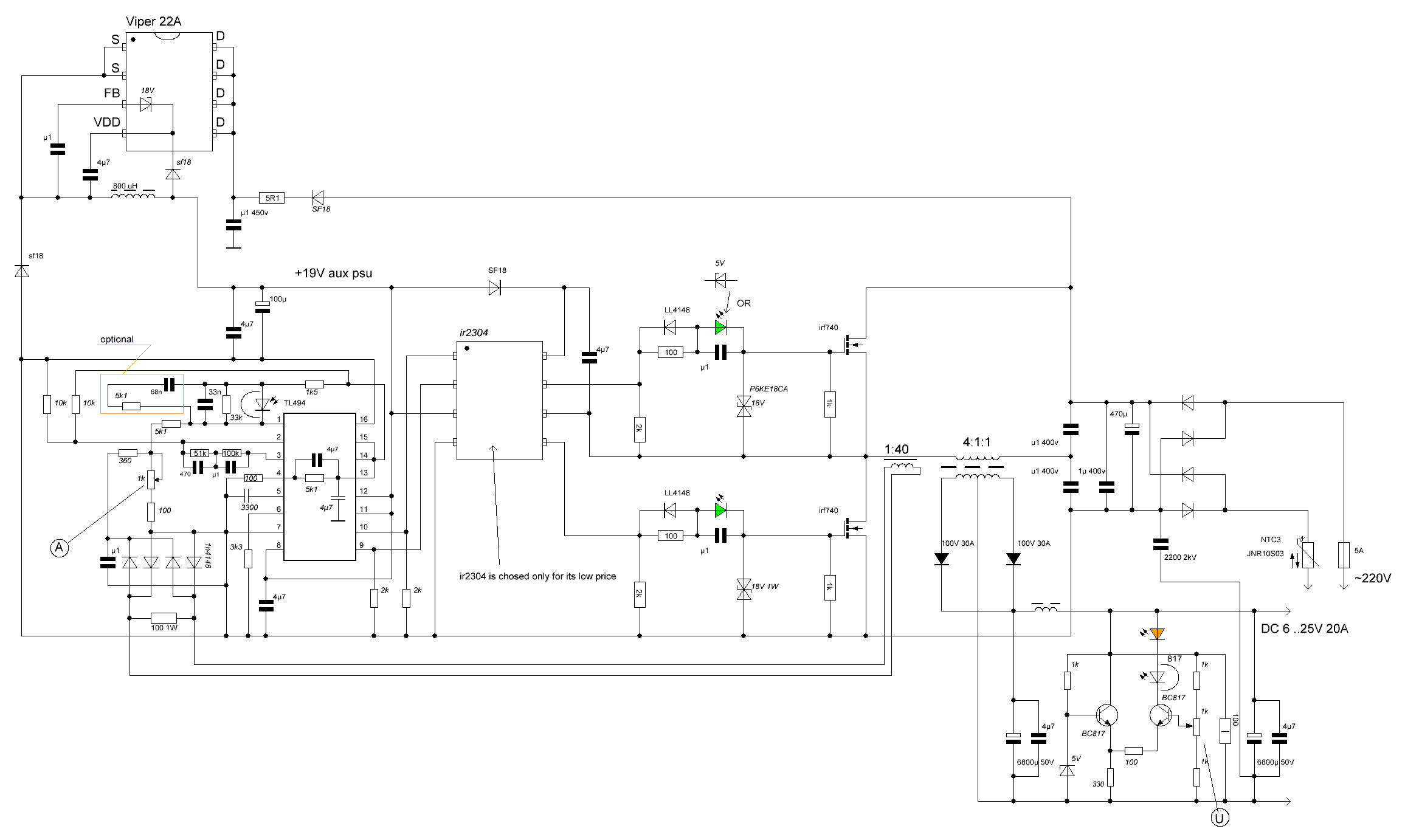
This is my 15V 10A Hlaf Bridge SMPS DSC01367.JPG
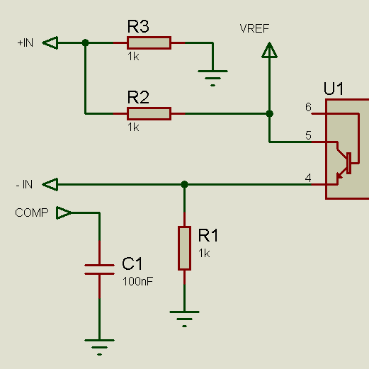
Here are some measurements and the schematic
X.pngDSC01360.JPGDSC01361.JPGDSC01359.JPG

this project is not completed, as it has no feed back.
i can adjust the output voltage using the dead time control of the tl494.

Before listing my problems, Any Notes about the scheme or the circuit ?

Now, my problems are:
1) The Output Filter "LC".
The output of the PS suffering from some ripples and i cant eliminate them using the filter circuit
i tried to use the formulas of output filter of my book "POWER SUPPLY COOKBOOK Marty Brown"output filter formula.png
but there are alot of ripples in the output.
can i use snubber circuit across the transformer secondary side to solve this problem? or what can i do to solve the problem?

2) The feedback
i tried to make isolated feedback but there are some problems.

I prefer to solve the first problem before starting the 2nd problem details.

thanks in advance,
Hz
 

First of all, your schematic lacks a freewheeling diode on the secondary side. That would definitely cause problems with the output waveform.

Looking at the last scope trace, it looks like that "ripple" is just EMI coupling from the switching nodes to the scope probe. That interference might not actually exist on the output, and could just appear due to poor probing.

For the ringing on the primary circuit, you could try using some simple RC snubbers. But generally you'd have much better luck using an etched PCB with an optimized layout. Getting good results on perfboard is difficult.
 

thank u mtwieg

i want to know the connection of the freewheeling diode please (1 or 2) ??
**broken link removed**

any other notes ??

sorry, there is a problem in the attachment, here is the photo
shotkky connection.png
i want to know the connection of the freewheeling diode please (1 or 2) ??
also its rating ?

Thanks in advance,
Hz
 
Last edited:

Can any one help me ? :-(
 

Figure 1 shows the correct freewheeling diode connection. It's current will be about Iout*(1-D).
 
  • Like
Reactions: Hz2020

    Hz2020

    Points: 2
    Helpful Answer Positive Rating
Thank u mtwieg
Is that suitable ?? or it need some compensation else ??
DSC01375.JPG

i want to know also, is the filter capacitor is of the electrolyte type or ceramic unpolarized type ?

Then, I want to go to the second point " The Feedback "
1st) I want to design the feedback loop before starting the compensation
I made the design according to the example in page 129 in my book "POWER SUPPLY COOKBOOK Marty Brown" , I understand it well.
feedback.png
any errors ?
 

Thank u mtwieg
Is that suitable ?? or it need some compensation else ??
View attachment 85045That looks decent. As I said before, the bits of ringing seen there are likely coupled via EMI, so probing with a pigtailed ground lead will probably reduce them. Putting snubbers on the primary side of the transformer will also help.
i want to know also, is the filter capacitor is of the electrolyte type or ceramic unpolarized type ?
Either can work. Ceramics generally work better than standard aluminum electrolytics. Polymer aluminum capacitors also work quite well.
Then, I want to go to the second point " The Feedback "
1st) I want to design the feedback loop before starting the compensation
I made the design according to the example in page 129 in my book "POWER SUPPLY COOKBOOK Marty Brown" , I understand it well.
View attachment 85046
any errors ?
I'm don't think that circuit will work... The input voltage to the error amp isn't really well defined by the LED current, unless the phototransistor is saturated (which isn't a good thing in itself). I would recommend instead tying R4 from pin 1 to ground, then have the phototransistor tied from Vref (or some other positive bias) to pin 1.

Also you should check and make sure the loop feedback is negative. I think the way you're setting it up may be positive feedback.
 

Thanks mtwieg
I made a mistake while drawing the circuit
the actual circuit i want to draw was this
feedback true.png
I think it is right.
Any comments before starting the compensation ??
 

Yes that looks much more reasonable, and should have the correct feedback polarity as well. Looks like a good starting point, but of course you'll later have to add some sort of PI compensation scheme if you want good regulation.
 

Hi friends
After searching and reading and calculations i decide to make this feedback compensation circuit
final_feedback.png
but there is a problem
When the output voltage is below 15V (i use the dead time control to change Vout), The feedback has no action . Is that right ?
When Vout goes near the 15V a hear a noise and something goes wrong (the circuit will be damaged).
What is the problem that causes that noise ? And how to overcome this problem ?

please i need a help.

note i put a 20 ohm dummy load resistor to make a minimum output current of 750mA which used in the feedback design.

Thanks in advance,
Hz
 

What is the value of your output inductance? Is 750mA sufficient load?

How long after you hear the noise does the circuit get damaged? What gets damaged? Do the MOSFETs get shorted? Does any other component get damaged?

How loud is this noise? Does it have a high pitch? Does it seem to come from the transformer or the output inductor? Or some other component?

Common sources of audible noise are unstable feedback loops, insufficient output load (noise from the output inductor), loose/stray transformer windings (noise from transformer).
 

Thanks for reply Tahmid.
The output inductance is about 2mH. I put the 20 ohm load just as a dummy load but i can draw about 10A from that supply.

When i hear the noise (I think it from the transformer) and after about 2 seconds the fuse is burned and the MOSFETs burned also (shorted).

i think that only due to the feedback loop as when i remove the feedback loop and connect the compensation pin to the ground the circuit works properly (that of course after i changed all the burnt components).

Please help me to stabilize the feedback loop.

Thanks in advance,
Hz
 

For testing purpose, try this for the feedback connections:

9753518900_1357150770.png


Hope this helps.
Tahmid.
 

Pins 2-3 must not be shorted. You need to put a reference voltage on pin 2 and add a feedback circuit (R+C serie) between pin 2 and 3.
 

Thanks Friends
Thamid : the circuit is not work
there is no output (Vout=0) :-(
what should i do now ?
 

Did you connect exactly as I have shown? Did you connect the optocoupler LED side properly?

Measure the voltage on pin 1 and on pin 2. Post the measurements.
 

yes i connect it exactly.
there is no output voltage, so, the voltage of pin 1 and 2 equal zero

i expect that this circuit will not work as at the initial state the voltage at pin (IN+) = 2.5v, but the voltage at pin (IN-)=0 through the pull down resistor R1
so, the compensation pin (op amp output) will be high, and that will stop the clock source in the tl494

Am i right ???

Hz
 

Hi.
I think using optocoupler feedback in half - bridge converters without additional subterfuges possible only for chips with pulse-by-pulse shutdown feature, like UC3825 or SG3525.
However this scheme must be runnable -
 

Are there any method for opto isolated feedback instead of isolated transformer feedback as it require additional turns on the transformer? :-(

I want the concept of the design to think right.


However this scheme must be runnable -
when the load is changed . I think it will has no effect on the feedback voltage ????? please explain
 

Hi Deepone
Greetings. I have made both your smps both are working but VIPER 12A IC is dropping voltage to 8 volts. I am using TOP 244 for 15 volts DC to IR2153 IC. I am using T50 ferrite core voltage drop is 2 volts on 1000 W + 500W halogen T50 secondary is 70 0 70 AC. Mosfets used IRFP460 1 pair. I have tested with load for 1 hour mosfets barely luke warm. I used 47 ohms gate resistance. Now can I use IGBT for increased power and what is the gate resistor value for IGBT. Some pictures to show my work. Rough PCB I designed but once everything is okay better PCB will be designed. Thank you for all your cooperation and advice. Last I want to ask you which is better T50 core or ETD59. Many thanks for your wonderful schematic and help.

Warm Regards
Andrew Lebon and Sameerx1
 

Attachments

  • DSCN3713 [Desktop Resolution].JPG
    DSCN3713 [Desktop Resolution].JPG
    664.6 KB · Views: 79
  • DSCN3732.jpg
    DSCN3732.jpg
    133.6 KB · Views: 78
  • DSCN3731.jpg
    DSCN3731.jpg
    123.7 KB · Views: 89

Status
Not open for further replies.

Similar threads

Part and Inventory Search

Welcome to EDABoard.com

Sponsor

Back
Top