Continue to Site

Welcome to EDAboard.com

Welcome to our site! EDAboard.com is an international Electronics Discussion Forum focused on EDA software, circuits, schematics, books, theory, papers, asic, pld, 8051, DSP, Network, RF, Analog Design, PCB, Service Manuals... and a whole lot more! To participate you need to register. Registration is free. Click here to register now.

SMD code marking help

diablo2

Newbie
Joined
Nov 25, 2023
Messages
4
Helped
0
Reputation
0
Reaction score
0
Trophy points
1
Activity points
39
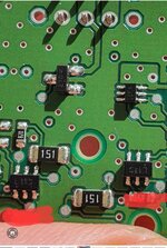
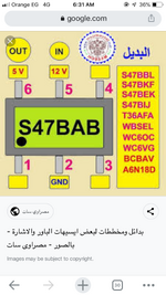
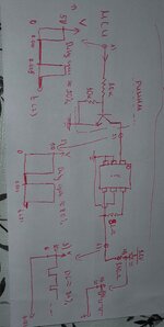
Hello, I've been trying to find what the part behind this smd code is "L1 s 47, but without much of a success. I think it's possibly a npn transistor or some sort of led driver packaged. I have attached a photo of the marking. Every help will be much appreciated!
 

Attachments

  • Screenshot_20231124-102417_Gallery.jpg
    Screenshot_20231124-102417_Gallery.jpg
    509.8 KB · Views: 85
Can be voltage regulator also, or step down voltage converter
From 12v to 5v , you can check the gnd pin if it’s gnd in your circuit or no, also the input voltage exist or no?

If not , then it might be dual transistor
 

Attachments

  • 0009A8B6-C49C-4140-B108-5CFD6BFA9F9C.png
    0009A8B6-C49C-4140-B108-5CFD6BFA9F9C.png
    815.1 KB · Views: 52
Thank you for your answers guys. The chip very much looks like some sort of a Npn device, but its connection in the circuit literally doesn't match anything I was able to find that matches this Smd code. I've drawn a simple schematic of how it appears to be connected. Any more suggestions are much appreciated!

20240130_092317.jpg
 
Hi,

have you measured the connections on a functional IC or by testing the defective one? For me it's not obvious where pin #5 is connected to, and by testing/measuring on the faulty IC, the GND connection might not be correct. I would recommend to desolder the IC and show us a picture and measure again.

It might be some (complementary) bipolar transistor pair to increase current handling capability e.g. Sziklai Pair, but here I would miss a base connection. Further, is there a series element i.e. a resistor along pin #1? If this is the base of a bipolar transistor, the base current has to be limited.

What is the frequency, duty cycle and amplitude of your PWM?

BR
 
Hi,
The continuity was done on a functional ICs, in fact there was 4 in total I checked it on, which are driving each side of a RGBW led. On the question about what's connected before pin #1, there actually are 2x PUMH11 (dual npn package) with each branch driving one of the 4x ICs. And if we question what actually drives those PUMH11, I think it was a 5V, 200Hz,low duty-cycle signal coming from a MCU. Not sure how useful that info would be. Also, although it would have been nice if the exact model is found, if I could I find a similar spec npn with some trial and error, might still work for me.

Thanks again!
 
Hi,

in general it's not that easy to perform a reliable in-circuit test of an IC. But for the GND connection of pin #5, on a "good" IC that should work.
You could desolder one of the good ICs and teest it with a multimeter, if i tis really a dual bipolar transistor pair [1].

But with your last statement of the additional NPN transistors (PUMH11) I'm rather confused how the actual connection looks like. The below sketch would match your verbal discription (somehow), but it doesn't make sense to me. You also mentioned the PWM is comming from the MCU, how is it connected to the PUMH11? I would miss some pullup at the pin #1/collector of the PUMH11 for the sketch below. Otherwise, I would assume the PWM has a HIGH level voltage of 12V. How does the signal at node XX looks like, is it matching the PWM singal at pin #1 of the IC, or is it inverted?

Could you show us a more detailed sketch, also including the HIGH level voltage level of your PWM singal (at XX and pin#1), as well as the frequeny and duty cycle?

LED_DRIVER_.png


[1] https://www.wikihow.com/Test-a-Transistor

BR
 
Hi,
I will take your advise and desolder and measure one of those on Monday as I left the board at work...

Regarding the rest, I agree that it's rather confusing. Not sure if it makes sense to be designed that way, but it came to my mind the unknown element might be a pnp device with internal base-emitter bias resistor. I'm not sure really. I've managed to dig out some scope images which I made when I initially tested the board in the car while plugged. I hope you can read smth from it.
 

Attachments

  • 20240217_194114.jpg
    20240217_194114.jpg
    1.6 MB · Views: 30

LaTeX Commands Quick-Menu:

Similar threads

Part and Inventory Search

Welcome to EDABoard.com

Sponsor

Back
Top