Continue to Site

Welcome to EDAboard.com

Welcome to our site! EDAboard.com is an international Electronics Discussion Forum focused on EDA software, circuits, schematics, books, theory, papers, asic, pld, 8051, DSP, Network, RF, Analog Design, PCB, Service Manuals... and a whole lot more! To participate you need to register. Registration is free. Click here to register now.

Small signal S-parameter measurements of RF power amplifier using VNA

Status
Not open for further replies.

Mabrok

Full Member level 4
Joined
Mar 1, 2017
Messages
223
Helped
0
Reputation
0
Reaction score
1
Trophy points
18
Activity points
1,597
Hi,

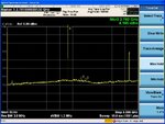
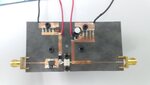
During my measurements for an RF power amplifier. Once I biased the device, I see overloaded on VNA screen. What can make this overloaded?


Note: My device consider as high power amplifier (Pout= 40 dBm), and I have used an attenuator of 20 dB between the output of the amplifier and port 2 of VNA.
 

Pout=+40dBm - 20dB attenuation = +20dBm VNA input power
+20dBm is the maximum input power for most of the VNAs on the market. I would recommend to add at least another 10dB of attenuation.
 

Hi. How did you decide 20 dB attenuation is enough for your setup? 20 dBm of power is considered high and even dangerous for many instruments.
Use at least 40 dB of attenuator in your tests.
First, check your PA with a spectrum analyzer to make sure its stability.
Do you have DC at the output? If so, make sure your instruments are tolerant to that DC level or provide appropriate DC blocking.
 

Don't risk damaging a $10K+ instrument. Put enough attenuation such that it will be safe even if the RFPA gives 10dB higher than its max rating. 40dB should be enough, and won't significantly degrade accuracy of S21 measurements.

If you want to measure S12 or S22, then you will need to invest in a load pull setup.
 

PA may oscillate.. Take this into account.
+20dBm may not damage the VNA but it saturates its Input Circuit.Best choice is to use -10dBm as a rule of thumb.
Not less than that level because optimum measurement uncertainty is around this point for most of VNAs.
 

    Mabrok

    Points: 2
    Helpful Answer Positive Rating

    Georgy.Moshkin

    Points: 2
    Helpful Answer Positive Rating
Hi. How did you decide 20 dB attenuation is enough for your setup? 20 dBm of power is considered high and even dangerous for many instruments.
Use at least 40 dB of attenuator in your tests.
First, check your PA with a spectrum analyzer to make sure its stability.
Do you have DC at the output? If so, make sure your instruments are tolerant to that DC level or provide appropriate DC blocking.
I used 20 dB attenuator because it is the only one available in my lab. My VNA max input power 26 dBm. So, I think 20 dB attenuator is enough (40-20= 20 dBm).
How I can check the stability with spectrum analyzer? Can you please explain more?
Regarding the DC, I already used appropriate DC block at the input and output.
 

How I can check the stability with spectrum analyzer? Can you please explain more?
Adjust Bandwidth to maximum ( it should have 30GHz or whatsoever..) and decrease RBW to minimum or closer value to observe low level oscillations.
And check oscillations if there are without any Input Signal applied.Don't forget to insert an appropriate attenuator btween PA Output and SA otherwise the PA may roast your SA.And decrease this attenuator step by step slowly unless there is no explicit oscillation.
 

"Without any input signal applied": Do you mean to switch off RF input at the signal generator but still connecting the cable from SG to the amplifier's input?
 

"Without any input signal applied": Do you mean to switch off RF input at the signal generator but still connecting the cable from SG to the amplifier's input?
Yes.. If there is an oscillation, you'll able to see it without any RF Input.
 

    Mabrok

    Points: 2
    Helpful Answer Positive Rating
Yes.. If there is an oscillation, you'll able to see it without any RF Input.
To ensure the stability, should have no oscillation in and out of band (0-30 GHz)? or only in band of interest (3.4-3.6 GHz)?
 

Yes.. If there is an oscillation, you'll able to see it without any RF Input.
This after I check the stability with spectrum analyzer.
 

Attachments

  • power.JPG
    power.JPG
    115.8 KB · Views: 176

As I said.. There is an oscillation at 2.7GHz.Ensure the stability is well maintained then continue to measure.Otherwise VNA will always be saturated by this oscillation signal ( fortunately it's small amplitude, it might have very strong so might blow up the VNA..) and measurements will be impossible.
In regard of signal amplitude, oscillation-I think- osccurs at the Output Side.If it was at Input Side, the amplitude would be higher.
 

    Mabrok

    Points: 2
    Helpful Answer Positive Rating
As I said.. There is an oscillation at 2.7GHz.Ensure the stability is well maintained then continue to measure.Otherwise VNA will always be saturated by this oscillation signal ( fortunately it's small amplitude, it might have very strong so might blow up the VNA..) and measurements will be impossible.
In regard of signal amplitude, oscillation-I think- occurs at the Output Side. If it was at Input Side, the amplitude would be higher.
How there is an oscillation at 2.7 GHz and the signal looks like smooth at this frequency if we compare it with rest of frequencies where there is many spikes?
 

Adjust Bandwidth to maximum ( it should have 30GHz or whatsoever..) and decrease RBW to minimum or closer value to observe low level oscillations.
And check oscillations if there are without any Input Signal applied.Don't forget to insert an appropriate attenuator btween PA Output and SA otherwise the PA may roast your SA.And decrease this attenuator step by step slowly unless there is no explicit oscillation.
By using this method. Could you please explain clearly how I can Identify the oscillation in the signal observed on the SA screen?
 

Not sure how else to explain it. A stable amplifier with no input signal should only produce noise (and maybe power supply ripple) on its output. But your SA shows a clear tone at 2.7GHz. This implies oscillation, as there's no other plausible explanation for the tone.

The SA plot doesn't really give any insight into why the oscillation occurs, but it does show it exists. The VNA is better suited to debugging oscillations, but only if you can measure all four network parameters. But if you try to measure S22 or S12 by connecting the amplifier output directly to the VNA, then you will very likely end up destroying the instrument.
 

    Mabrok

    Points: 2
    Helpful Answer Positive Rating
Not sure how else to explain it. A stable amplifier with no input signal should only produce noise (and maybe power supply ripple) on its output. But your SA shows a clear tone at 2.7GHz. This implies oscillation, as there's no other plausible explanation for the tone.

The SA plot doesn't really give any insight into why the oscillation occurs, but it does show it exists. The VNA is better suited to debugging oscillations, but only if you can measure all four network parameters. But if you try to measure S22 or S12 by connecting the amplifier output directly to the VNA, then you will very likely end up destroying the instrument.
Yes that is why i used the SA to measure the stability. As with VNA, I use 40 dB attenuator between the output of the amplifier and port 2 of VNA. In this case S12 and S22 will not be accurate. As a result, can not calculate K-stability factor to ensure the stability.

How if I remove the external attenuator, and set the internal attenuator of the VNA. Will S12 & S22 be accurate?
Theoretically, if the S parameters of the attenuators and cables are known, you can disembed the true S parameters of the DUT using the measured S parameters from the VNA. But this becomes very difficult as the attenuation rises, a practical limitation is probably 10dB.

Whether the attenuation is external or internal doesn't really matter. But I doubt the built-in attenuators on your VNA will stand up to your unstable DUT.
 

    Mabrok

    Points: 2
    Helpful Answer Positive Rating
Theoretically, if the S parameters of the attenuators and cables are known, you can disembed the true S parameters of the DUT using the measured S parameters from the VNA. But this becomes very difficult as the attenuation rises, a practical limitation is probably 10dB.

Whether the attenuation is external or internal doesn't really matter. But I doubt the built-in attenuators on your VNA will stand up to your unstable DUT.
Can the poor layout causes this oscillation? Especially the DC ground connection as I have used square batch with one centered hole for ground connection through metallic screw. I have saw in some PA layout they use symmetrical array of hole.
Attached picture is my PCB.
 

Attachments

  • ٢٠٢٠١٠١٦_١٦١٩٤٨.jpg
    ٢٠٢٠١٠١٦_١٦١٩٤٨.jpg
    1.1 MB · Views: 184

Biasing lines do not look good. If those are 50 Ohm SMA connectors, microstrip looks too thin. Probably it is better to put input and output biasing farther away. I really would recommend to order some generic FR4 1.0mm boards manufactured at PCB fab based on your layout, with nice vias and everything, and you can put several prototypes on a single board, and obtain good results much easier. You can even put some resonator and estimate dielectric constant. I do not see what transistor do you use. I only familiar with low power FETs, many of them usually are stable if terminated with 50 Ohm (unstable circle boundaries are very far from center) and source pin is grounded very well with VIAS on a relatively thin substrate, for example 1.0mm or thinner FR4. Same transistors oscillate easily if termination is far from 50 Ohm, or there is bad grounding, when substrate is too thick and/or vias are too far from source pins, unstable circles are quickly "moved" to the center of Smith chart.
I would use radial quarter wave stubs for biasing, use thinnest possible biasing lines. On FR4 with Er=4.5 H=1.0mm main 50Ohm line width is 1.85mm. Biasing line may be around 0.3mm thick, quarterwave length between 50Ohm line and radial stub will be 18mm.
The only problem would left is finding good capacitors for DC blocking, or using special ones which are pretty expensive.

Possible design:
1) 4x4cm ground area around transistor on top layer, with many vias around source pins. Input and output lines are GCPW lines.
2) rounded transition from GCPW to microstrip on the edges of 4x4cm ground area. Both for input and output.
3) 0.2 mm thin biasing lines with radial stubs.
4) commercial DC block capacitors somewhere near SMA connectors.
On a FR4 substrate at 2.4GHz it will perform pretty the same even if Er will be 3.5 or 5.5, with or without solder mask, with high or low dielectric losses. Phase length and characteristic impedance do not change much at 2.4GHz. You probably will get more differences from how SMA connectors and transistor was soldered. If every component is ok and layout arrangement is good, and you checked stability circles, then there will be no impedance "swirling" around Smith chart through unstable regions of transistor as dielectric constant changes or if you connect SMA cables with different length or something like that.
Large copper area around transistor will help to dissipate more heat, putting thin biasing lines away from transistor gives lower temperature and higher possible currents (https://www.eeweb.com/tools/external-pcb-trace-max-current/), minimizes input to output coupling and forming of unwanted parallel feedback oscillator.
 
Last edited:

    Mabrok

    Points: 2
    Helpful Answer Positive Rating
Status
Not open for further replies.

Part and Inventory Search

Welcome to EDABoard.com

Sponsor

Back
Top