Continue to Site

Welcome to EDAboard.com

Welcome to our site! EDAboard.com is an international Electronics Discussion Forum focused on EDA software, circuits, schematics, books, theory, papers, asic, pld, 8051, DSP, Network, RF, Analog Design, PCB, Service Manuals... and a whole lot more! To participate you need to register. Registration is free. Click here to register now.

sine wave from AD9833 with SPI using PIC18F4580

Status
Not open for further replies.

syamin0712

Member level 1
Joined
Jan 2, 2015
Messages
36
Helped
0
Reputation
0
Reaction score
0
Trophy points
6
Activity points
406
Hi everyone,
I need some help for those who have experience in generating sine waveforms using AD9833 and PIC18F4580.

This is my first experience using SPI to code the sine waveform from PIC18F4580 as a master and AD9833 as the slave.

I set the pin between PIC18F4580 and AD9833 as follows:

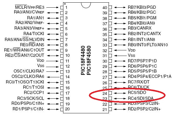
RC4/SDI/SDA ---- SDATA
RC3/SCK/SCL ---- SCLK
RA5/SS ---- FSYNC

Does it correct the pin that I set between PIC18F4580 and AD9833?

To generate the 2MHz: By using the formula in AD9833 data sheet page 15, while assuming MCLK is 40MHz. I have set the FREQ register to 13421773 decimal number (110011001100110011001101) in binary.

Also, is it correct the MCLK that I use if im using XTAL 10MHz and enable HSPLL so that it becomes 40MHZ?

Could anybody check what is wrong with my code?Here, Im using CCS C compiler to write my code.
Or is there any additional code that I have to write?

Code:
#device PIC18F4580 
//configure a 10MHz crystal to operate at 40MHz, // System setting - Use 10MHz XTAL with PLL. New Freq: 10MHz x 4 = 40Mhz. 
#fuses HS,NOWDT,NOPROTECT,NOLVP,NODEBUG 
#define OSC_PLL_ON 
#use delay(clock=10000000) 
#use spi(DO= PIN_C4 , CLK = PIN_C3, ENABLE = PIN_A5, BITS = 16, MASTER, ENABLE_ACTIVE = 0, MSB_FIRST, IDLE = 1) 

//DO=SDATA/SDA pin, 
//CLK=SCLK/SCK pin, 
//ENABLE=FSYNC/SS pin, 
//BITS=16 is max num of bit in one transfer is 16, 
//MASTER=PIC is master and AD9833 is slave, 
//ENABLE_ACTIVE = 0 is FSYNC pin is active low, 
//MSB_FIRST is accept MSB of each transfer first 
//IDLE=1 is FSYNC always high when not in use 


void main() 
{ 

   while(1) 
   { 
      // activate control register; both LSB & MSB FREQ write consequtively; enable reset; enable sinewaveform signal 
     spi_xfer(0b0010000100000000); 
    
     //on FREQ0 for generate 2MHz if using MCLK=40MHz ; 13421773 in decimal 
     spi_xfer(0b100110011001101);  
     spi_xfer(0b0100001100110011); 
      
     //on PHASE0 with zero phase shift 
     spi_xfer(0b1100000000000000);  
      
     //activate control register; both LSB & MSB FREQ write ; disable reset; enable sinewaveform signal 
     spi_xfer(0b0010000000000000); 
   } 

}


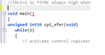
Here is the link for the screen after i compile my code

https://obrazki.elektroda.pl/9098671100_1440397794.png

When I compile these, two errors appear:
The function of #use spi shown an error
"USE parameter value is out of range. Not a number. PIN_C4"
and at void main() it shown "I/O error 131".

What is meant by that statement?
 
Last edited by a moderator:

I don know whether its a software or hardware SPI, but if its a hardware then wrong pin configuration and this pins are not remappable.

5790841200_1440399465.jpg


I already once worked with this IC for FM.

I don know your application but I think you needed to put delay between SPI writes, so that it will be meaning full.
 

#fuses HS,NOWDT,NOPROTECT,NOLVP,NODEBUG

Check if there is any fuses like HSPLL that you have to include.

#define OSC_PLL_ON

I think this doesn't make any difference.

#use delay(clock=10000000)

I think that when you use 4xPLL you have to mention the actual clock that you get after PLL here like.

Code:
#use delay(clock=40000000)


The device header contains these

Code:
////////////////////////////////////////////////////////////////// INTERNAL RC
// Oscillator Prototypes:
_bif int8 setup_oscillator(int8 mode);
_bif int8 setup_oscillator(int8 mode, signed int8 tune);
// Constants used in setup_oscillator() are:
// First param:
#define OSC_31KHZ   0
#define OSC_125KHZ  0x10
#define OSC_250KHZ  0x20
#define OSC_500KHZ  0x30
#define OSC_1MHZ    0x40
#define OSC_2MHZ    0x50
#define OSC_4MHZ    0x60
#define OSC_8MHZ    0x70
#define OSC_16MHZ   0x4060
#define OSC_32MHZ   0x4070
// The following may be OR'ed in with the above using |
#define OSC_TIMER1  1
#define OSC_INTRC   2
#define OSC_NORMAL  0
// The following may be OR'ed in with the above using |
#define OSC_IDLE_MODE  0x80
#define OSC_31250   0x8000
#define OSC_PLL_ON  0x4000
#define OSC_PLL_OFF 0
// A second optional parameter may be used with this part to fine
// tune the speed (signed int,-32 to 31)
// Result may be (ignore all other bits)
#define OSC_STATE_STABLE 4
#define OSC_STATE_EXT_RUNNING 8
 
Last edited:

I don know whether its a software or hardware SPI, but if its a hardware then wrong pin configuration and this pins are not remappable.

5790841200_1440399465.jpg


I already once worked with this IC for FM.

I don know your application but I think you needed to put delay between SPI writes, so that it will be meaning full.

What do you mean the hardware or software SPI?
AD9833 is the waveform generator ic and the 3 pin attached it (FSYNC, SDATA and SCLK ) have to link with SPI device. Here im using the PIC18F4580 as the SPI device.
My application is for electrical tomography field. I want to transmit 2MHz sine waveform from the ic AD9833 and will feed the signal to amplifier circuit before connected to the transmitter sensor.

Do you mean I have to put the delay for every single instruction of SPI write? or just before the code "while"?

- - - Updated - - -

Check if there is any fuses like HSPLL that you have to include.


I think this doesn't make any difference.


I think that when you use 4xPLL you have to mention the actual clock that you get after PLL here like.

Code:
#use delay(clock=40000000)

Hi,
actually I have tried to put the function HSPLL but it showed an error.
I tried search the way to give the correct function HSPLL but I couldnt find it.
When I check in the device support for PIC18F4580, there no word like HSPLL, its only have HS.

So, if gonna to use HSPLL; what is the correct approach that I have to use?
 

What do you mean the hardware or software SPI?

In hardware SPI module without remappable pins you cant use other pin for the same purpose.
The DO is actually PIN_C5 in the hardware but PIN_C4 in your code.

I want to transmit 2MHz sine waveform from the ic AD9833
If you want a single frequency why dont you use a analog crystal oscillator.

Do you mean I have to put the delay for every single instruction of SPI write? or just before the code "while"?
For a single frequency sine output you can send the frequency byte only one time and release the reset. for varying the frequency usually we will send in some particular delay timings. Here you don need to send them again and again through a while loop. You can just put the while loop in the bottom to get it working.
 

Where is the spi initialization code ? MCLK is the clock for AD9833. 10 MHz + 4xPLL = 40 MHz is for your PIC. I don't know whether you can supply 40 MHz for AD9833s MCLK.

The PIC18F4580 device header shows these functions for SPI. I assume you are using CCS C's SPI functions.

Code:
////////////////////////////////////////////////////////////////// SPI
// SPI Functions: SETUP_SPI, SPI_WRITE, SPI_READ, SPI_DATA_IN
// SPI Prototypes:
_bif void setup_spi(int32 mode);
_bif void spi_write(int8 value);
_bif int8 spi_read(void);
_bif int8 spi_read(int8 value);
_bif int1 spi_data_in(void);
_bif void setup_spi2(int32 mode);  
_bif void spi_write2(int8 value);  
_bif int8 spi_read2(void);  
_bif int8 spi_read2(int8 value);  
_bif int1 spi_data_in2(void);  
// Constants used in SETUP_SPI() are:
#define SPI_DISABLED             0x00
#define SPI_MASTER               0x20
#define SPI_SLAVE                0x24
#define SPI_SCK_IDLE_HIGH        0x10
#define SPI_SCK_IDLE_LOW         0x00
#define SPI_CLK_DIV_4            0x00
#define SPI_CLK_DIV_16           0x01
#define SPI_CLK_DIV_64           0x02
#define SPI_CLK_T2               0x03
#define SPI_SS_DISABLED          0x01

#define SPI_XMIT_L_TO_H          0x4000
#define SPI_XMIT_H_TO_L          0x0000

#define SPI_SAMPLE_AT_MIDDLE     0x0000
#define SPI_SAMPLE_AT_END        0x8000

//The following are provided for compatibility
#define SPI_L_TO_H       SPI_SCK_IDLE_LOW
#define SPI_H_TO_L       SPI_SCK_IDLE_HIGH

So, please show the full code and show the initialization of SPI module.


Code C - [expand]
1
#use spi(DO= PIN_C4 , CLK = PIN_C3, ENABLE = PIN_A5, BITS = 16, MASTER, ENABLE_ACTIVE = 0, MSB_FIRST, IDLE = 1)


In the image you posted it the DO appears in blue and I think the compiler is thinking it as Do of Do...WHILE() loop, a reserved word. So, use names like SPI_DO, SPI_CLK, etc... and try.


Edit:

In the image you posted it shows something strange. See attached image. There is a code

Code:
unsigned int16 spi_xfer(void)

between
Code:
void main()
and
Code:
while(1)

Is it a function prototype or a function definition. If yes, what is it doing in the void main() ?
 

Attachments

  • spi.png
    spi.png
    3.7 KB · Views: 104
Last edited:

Where is the spi initialization code ? MCLK is the clock for AD9833. 10 MHz + 4xPLL = 40 MHz is for your PIC. I don't know whether you can supply 40 MHz for AD9833s MCLK.

The PIC18F4580 device header shows these functions for SPI. I assume you are using CCS C's SPI functions.

Code:
////////////////////////////////////////////////////////////////// SPI
// SPI Functions: SETUP_SPI, SPI_WRITE, SPI_READ, SPI_DATA_IN
// SPI Prototypes:
_bif void setup_spi(int32 mode);
_bif void spi_write(int8 value);
_bif int8 spi_read(void);
_bif int8 spi_read(int8 value);
_bif int1 spi_data_in(void);
_bif void setup_spi2(int32 mode);  
_bif void spi_write2(int8 value);  
_bif int8 spi_read2(void);  
_bif int8 spi_read2(int8 value);  
_bif int1 spi_data_in2(void);  
// Constants used in SETUP_SPI() are:
#define SPI_DISABLED             0x00
#define SPI_MASTER               0x20
#define SPI_SLAVE                0x24
#define SPI_SCK_IDLE_HIGH        0x10
#define SPI_SCK_IDLE_LOW         0x00
#define SPI_CLK_DIV_4            0x00
#define SPI_CLK_DIV_16           0x01
#define SPI_CLK_DIV_64           0x02
#define SPI_CLK_T2               0x03
#define SPI_SS_DISABLED          0x01

#define SPI_XMIT_L_TO_H          0x4000
#define SPI_XMIT_H_TO_L          0x0000

#define SPI_SAMPLE_AT_MIDDLE     0x0000
#define SPI_SAMPLE_AT_END        0x8000

//The following are provided for compatibility
#define SPI_L_TO_H       SPI_SCK_IDLE_LOW
#define SPI_H_TO_L       SPI_SCK_IDLE_HIGH

So, please show the full code and show the initialization of SPI module.


[syntax]
#use spi(DO= PIN_C4 , CLK = PIN_C3, ENABLE = PIN_A5, BITS = 16, MASTER, ENABLE_ACTIVE = 0, MSB_FIRST, IDLE = 1)
[/syntax]

In the image you posted it the DO appears in blue and I think the compiler is thinking it as Do of Do...WHILE() loop, a reserved word. So, use names like SPI_DO, SPI_CLK, etc... and try.

Hi,

the code that I posted was my fully code. I thought that code was included the initialization for spi
Actually, I have refer to this link to build up my code since i dont have any experinece on it.
http://hades.mech.northwestern.edu/index.php/Waveform_Generation_with_AD9833,_and_SPI

is it wrong?or is there any simple way to code the sine wave?
 

In hardware SPI module without remappable pins you cant use other pin for the same purpose.
The DO is actually PIN_C5 in the hardware but PIN_C4 in your code.


If you want a single frequency why dont you use a analog crystal oscillator.


For a single frequency sine output you can send the frequency byte only one time and release the reset. for varying the frequency usually we will send in some particular delay timings. Here you don need to send them again and again through a while loop. You can just put the while loop in the bottom to get it working.

So, what is the correct way to link the FSYNC, SDATA and SCLK pin from AD9833 and the pin from PIC18F4580?
Analog oscillator device?SO, we no need to on the osc from pic?
 

I don't know whether you can supply 40 MHz for AD9833s MCLK.
Good question. Actually you can't for two reasons.
- AD9833 maximum MCLK specification is 25 MHz
- PIC18 has no option to output the PLL clock

More generally speaking, PIC PLL configuration has nothing to do with DDS frequency. To safe a separate crystal oscillator for the AD9833, you could run the PIC with a 20 or 25 MHz crystal or crystal oscillator.
 

Where is the spi initialization code ? MCLK is the clock for AD9833. 10 MHz + 4xPLL = 40 MHz is for your PIC. I don't know whether you can supply 40 MHz for AD9833s MCLK.

The PIC18F4580 device header shows these functions for SPI. I assume you are using CCS C's SPI functions.

Code:
////////////////////////////////////////////////////////////////// SPI
// SPI Functions: SETUP_SPI, SPI_WRITE, SPI_READ, SPI_DATA_IN
// SPI Prototypes:
_bif void setup_spi(int32 mode);
_bif void spi_write(int8 value);
_bif int8 spi_read(void);
_bif int8 spi_read(int8 value);
_bif int1 spi_data_in(void);
_bif void setup_spi2(int32 mode);  
_bif void spi_write2(int8 value);  
_bif int8 spi_read2(void);  
_bif int8 spi_read2(int8 value);  
_bif int1 spi_data_in2(void);  
// Constants used in SETUP_SPI() are:
#define SPI_DISABLED             0x00
#define SPI_MASTER               0x20
#define SPI_SLAVE                0x24
#define SPI_SCK_IDLE_HIGH        0x10
#define SPI_SCK_IDLE_LOW         0x00
#define SPI_CLK_DIV_4            0x00
#define SPI_CLK_DIV_16           0x01
#define SPI_CLK_DIV_64           0x02
#define SPI_CLK_T2               0x03
#define SPI_SS_DISABLED          0x01

#define SPI_XMIT_L_TO_H          0x4000
#define SPI_XMIT_H_TO_L          0x0000

#define SPI_SAMPLE_AT_MIDDLE     0x0000
#define SPI_SAMPLE_AT_END        0x8000

//The following are provided for compatibility
#define SPI_L_TO_H       SPI_SCK_IDLE_LOW
#define SPI_H_TO_L       SPI_SCK_IDLE_HIGH

So, please show the full code and show the initialization of SPI module.


Code C - [expand]
1
#use spi(DO= PIN_C4 , CLK = PIN_C3, ENABLE = PIN_A5, BITS = 16, MASTER, ENABLE_ACTIVE = 0, MSB_FIRST, IDLE = 1)


In the image you posted it the DO appears in blue and I think the compiler is thinking it as Do of Do...WHILE() loop, a reserved word. So, use names like SPI_DO, SPI_CLK, etc... and try.


Edit:

In the image you posted it shows something strange. See attached image. There is a code

Code:
unsigned int16 spi_xfer(void)

between
Code:
void main()
and
Code:
while(1)

Is it a function prototype or a function definition. If yes, what is it doing in the void main() ?

the strange code appeared between the void main and the while() was just i try and error
 

I don't know whether you can use the 10 Mhz crystals's clock used for PIC to provide clock the MCLK pin of AD9833. Try to use a dedicated clock (crystal) for AD9833 and see if that works.

Edit:

In the link you provided he mentions that MCLK of AD9833 can be tied to Oscillator of PIC but he doesn't mention the crystal frequency used for PIC. According to datasheet of AD9833 I think you can't have a clock more than 25 MHz for the AD9833's MCLCK
 

"To safe a separate crystal oscillator for the AD9833, you could run the PIC with a 20 MHz crystal."

Do you mean I just need the same crystal for PIC and AD9833 which is 20MHz?I mean only one crsytal that connected at pin RA7 and RA6 on PIC18F4580 and the pin RA7 or RA6 is connected to the MCLK on the AD9833?
 

Yes.

Use a 20 MHz crystal for PIC on it OSC1 and OSC2 pins with two 22pF Ceramin Capacitors. For fuses use HS. Connect OSC1 pin of PIC to MCLK of AD9833.

If you can provide the link which gives info related to your spi_xfer() function then I can help you more. Maybe it is a spi function used to transmit 16 or 32 bits of data at once.
 

There's no input level specification for MCLK, so the clock signal should have sufficient swing. This will surely work with a crystal oscillator and hopefully with OSC2 (RA6) when using a crystal in HS mode.
 

Status
Not open for further replies.

Similar threads

Part and Inventory Search

Welcome to EDABoard.com

Sponsor

Back
Top