Continue to Site

Welcome to EDAboard.com

Welcome to our site! EDAboard.com is an international Electronics Discussion Forum focused on EDA software, circuits, schematics, books, theory, papers, asic, pld, 8051, DSP, Network, RF, Analog Design, PCB, Service Manuals... and a whole lot more! To participate you need to register. Registration is free. Click here to register now.

Simulation and Hardware mismatch

Status
Not open for further replies.

anushaas

Member level 5
Joined
Jan 4, 2011
Messages
84
Helped
0
Reputation
0
Reaction score
0
Trophy points
1,286
Activity points
1,979
Hi

The following circuit was simulated using Tina 9 and the hardware implementation for the same was done on an NI Elvis II+ board
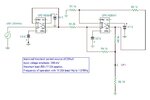
AD8041.JPG

The frequency response of the circuit with load resistance R6 as 10k on simulation gave a -3dB gain at 7.8MHz as shown below

Bodeplot_Buffer_10 kload.jpg

However the same on implementation gave a -3dB gain at 630.957kHz approx.The response obtained is as shown below
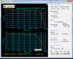
Bode_Buffer_10k load.png

The response (simulation and hardware) for R6 as 10Ohm is as shown below:
Bodeplot_Buffer_10 Ohm load.jpg

Bode_Buffer_10Ohm load.png

I understand that practical implementation will involve parasitic capacitances in the circuit but will the variation be this much?
 

I will try that.I am already using a 6.8 pF across R2. Sorry, that is not shown in the circuit schematic.
 

try 10 pf across R3 or R4.. assuming low inductive layout and R6 is not WW.

R6 is not wirewound.It is a carbon film resistor of 10k.

I tried the above circuit with a 10pF across R3 (6.8pF across R2 was removed).The frequency response obtained during simulation and hardware implementation is as shown below:

Simulation:
**broken link removed**

Response for Hardware:
**broken link removed**

The same circuit with 10pF across R4(alone) gave the following response

Simulation:
**broken link removed**

Hardware:
**broken link removed**

In both cases the load resistance was 10k.A 10pF across R4 was giving a -3dB frequency slightly less than 1MHz but the hardware implementation showed a dropping gain with frequency while simulation showed a rising gain.Why is it so?
 

To give us an idea of the analyzer frequency response, can you please also show the output of the first amplifier stage?
 

To give us an idea of the analyzer frequency response, can you please also show the output of the first amplifier stage?


Here it is.
The circuit is as shown below.VF1 is now the output of first amplifier stage

Pic1.JPG

The frequency response on simulation is:
Bode_Buffer.jpg

Response from hardware implementation:
Bode_Buffer.png
 

O.K. Shows that the 0.5 dB drop at low frequency is appparently an instrument artefact, but it's basically measuring correctly up to 5 MHz.

So the 600 kHz cut-off in your measurements is a real hardware effect. I continue to assume that it's caused by a capacitance of about 25 pF parallel to your load, mainly the input capacitance of the measurement system and some additional circuit capacitance.

The issue has been already discussed in your previous thread. https://www.edaboard.com/threads/341771/ I wonder why you rescheduled the question without considering the previous discussion.

I did consider that.The probes used for measurement were properly compensated.I don't know what else to do.I suppose that the breadboard capacitance would be 2pF approx. and that definitely will not cause a 25pF parallel to load.
The NI Elvis scope channel has an input impedance of 1MOhm with 21pF capacitance.The measurement circuitry is as shown below:

**broken link removed**

I am using channel 0 for input and channel 1 for output.

Could this capacitance cause an error/But how can we get rid of it?
 

I don't know where the load capacitance is situated. You have about 12 pF probe capacitance plus some breadboard parasitics. So a 1 MHz bandwidth limitation can be expected anyway. But there seems to be 8 pF or so extra. I'm unable to localize it from a distance.

The NI 21 pF input capcitance specification explains at least the 0.5 dB gain step at 1 kHz. It happens because TPP0200 can't be compensated for > 18pF instrument capacitance, you would need TPP0201 in this case.

The best way to measure the real circuit bandwidth is to place a +1 OP buffer between current source and probe..
 

Might I suggest to check the 'scope (if this is indeed a
real oscilloscope behind the LabView curtain) BW limit
switch position, or the BW limitations of your particular
equipment?
 

The measurement in post #6 suggests that specified 5 MHz bandwidth of the measurement system is achieved, apart from a minor (0.5 dB) probe calibration error.
 

Status
Not open for further replies.

Similar threads

Part and Inventory Search

Welcome to EDABoard.com

Sponsor

Back
Top