Continue to Site

Welcome to EDAboard.com

Welcome to our site! EDAboard.com is an international Electronics Discussion Forum focused on EDA software, circuits, schematics, books, theory, papers, asic, pld, 8051, DSP, Network, RF, Analog Design, PCB, Service Manuals... and a whole lot more! To participate you need to register. Registration is free. Click here to register now.

Simple voltage mixer

Status
Not open for further replies.

Josato

Newbie level 4
Joined
Oct 4, 2011
Messages
6
Helped
0
Reputation
0
Reaction score
0
Trophy points
1,281
Activity points
1,349
Hi,

For an application, I want to mix a voltage waveform in cadence. You should be able to see it here: https://docs.google.com/open?id=0B0T5dH2mGd3vYlZ4cExCcEp2QXM

I tried to upload it using 'add an image', but it just hung forever for some reason.

The output of my circuit must be +-2v and ideally use no more than two opamps.

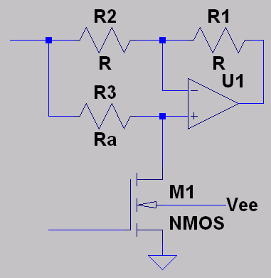
What I am trying to do is mix the modulated waveform seen in the upper left by the original high frequency wave. When the modulated wave you can see would go below 0v I switch one mosfet on and the other off into the differential amplifier, thus giving me a gain of 1 or -1. The desired output and circuit can be seen at the bottom. However, this output is in the range of milivolts, which is why I am using my opamp buffer to also give the voltage some gain before it is switched. However, the output ends up like the waveform in the top right.

I don't know how to get my output wave. I feel I am close, but I have a problem I can't figure out. As well as this, if you look closely at the waveform on the bottom (almost ideal one), the MOSFETS are not stopping the voltage at exactly 0v, it is spiking a bit. Additionally, if you look closely (I hope you can download this image) the normal and rectified wave don't have exactly the same gain. You can see that every odd peak is slightly less than it should be.

I tried for a very long time to figure out or find a circuit that could do this for me. If anyone could give a suggestion as to why mine is not working or a better method to use I would be extremely grateful

Thanks,

Jo
 

Many informations missing, e.g. frequency, FET type, magnitude and waveform of the demodulating signal. It looks like you have much crosstalk of original signal. May be a matter of FET Cds capacitance, missing bulk bias or unsuitable demodulation signal magnitude.

I guess the "desired output" has been generated by using ideal switches or a behavioral multiplier?

Wow, I thought I might have some missing information, but...
Thanks for the fast reply too!

Ok,

frequency of modulating signal: 50kHz - 90kHz (in this case 50)
frequency of modulated signal: 200 - 2000Hz (in this case 2000Hz)
FET - MOSFET n type (p type available) L = 0.8u W = 30u M = 1

The desired output was created using the circuit shown (although the negative waveform isn't good). However, it is on the scale of mV.

This is the whole block: https://docs.google.com/open?id=0B0T5dH2mGd3vVVhaSmFYVVFtMU0

The aim is to measure the capacitance of a plate (for a MEMS device). The inputs to the XY blocks are the displacement of a plate suspended parallel between two plates. As the center plate moves up and down the capacitance of between the center plate and the top plate varies, as does the cap. between center and bottom.

Applying a sinusoidal voltage to the top of the capacitive potential divider, and it's inverse to the bottom will give an output waveform whose magnitude varies with the capacitance. When the two capacitances are equal, the voltage between them should be 0v.

Thus, the output is as seen in the first post. Now, if the 'modulating' waveform is used to give a gain of 1 when it is positive and -1 when it is negative, we can get a wave that can be simply filtered to extract the data.

Do let me know if I am explaining things clearly.

EDIT: The real ideal behavior (not shown) I originally simulated using a behavioral multiplier and low-pass ABM. In that scenario I achieved near-perfect output.
 

I think, the main problem is that the control voltage doesn't switch the FETs fully on and off. Floating bulk connection is possibly an additional problem. You should verify correct operation of the demodulator with simple signals.

Are you designing an IC or a discrete circuit? In the former case, you should refer to a known analog switch topology, in the latter use an industry standard switch IC.

A synchronous demodulator (+/- 1 sign multiplier) can be made with an OP and a single ground referenced FET switch, which simplifies correct gate control signal generation.
 
  • Like
Reactions: tpetar

    tpetar

    Points: 2
    Helpful Answer Positive Rating
I think, the main problem is that the control voltage doesn't switch the FETs fully on and off. Floating bulk connection is possibly an additional problem. You should verify correct operation of the demodulator with simple signals.

Are you designing an IC or a discrete circuit? In the former case, you should refer to a known analog switch topology, in the latter use an industry standard switch IC.

A synchronous demodulator (+/- 1 sign multiplier) can be made with an OP and a single ground referenced FET switch, which simplifies correct gate control signal generation.

Hi, thanks for your reply.

Hmm, well I thought that the control voltage would switch the FETs. I am simply using an ABM at the moment to turn the signal into a square wave of 1v to 0v. Increasing it to more than 1v does not help. The bulk I thought was connected, although there is some gap between it's pins and the line I suppose. Connecting it doesn't do anything.

IC/discrete - well, whatever works I am going to be happy with to be honest. Looking around, is this what you mean: https://goo.gl/Y7OZ0 ? (Except instead of ground -2.5v) or here: https://goo.gl/iFOMx

I also read that using a 'dummy transistor' might help matching.

I am sorry, I don't fully get what you mean bu the 'OP and ground referenced switch'. Is there a schematic I can see?
 

I'm was just guessing about the problem. Intelligent usage of the circuit simulator should help to find out the actual reason.

I meaned a sign multiplier like below. In case of a MOSFET switch, the bulk should be still negative biased to process bipolar input voltages linearly.

1649182800_1353436321.gif
 

Hi,

Do you have typical values for the resistors I can try? I am getting very odd output at the moment. I am applying 1v square wave to the MOSFET. Also, is there a name for this circuit?

- - - Updated - - -

I meaned a sign multiplier like below.

It appears to work! (well, a variation of it) : https://docs.google.com/open?id=0B0T5dH2mGd3vMEw2VjJJWi1rQTA

I am applying 0 - 2.5v to the MOSFET.

THANK YOU VERY MUCH!
 

Hi,

Just to finish things off... Do you know what the name of this circuit is, if it has one? Or what the principle of operation is (it seems to be switching between inverting and non-inverting mode)? I would like to be able to write up the op amp and reference it as part of my report.

Regards,

Jo

EDIT: Also, why do I tie the bulk of the MOSFET to -2.5? Surely linearity isn't needed when it's acting as a switch (although it breaks when I take it off)
 
Last edited:

My suggestion is sign-multiplier, as already mentioned. In Horowitz, The Art of Electronics - 2nd Edition, the circuit can be found as exercise under the title "optional inverter", without much explanation.
 
  • Like
Reactions: Josato

    Josato

    Points: 2
    Helpful Answer Positive Rating
My suggestion is sign-multiplier, as already mentioned. In Horowitz, The Art of Electronics - 2nd Edition, the circuit can be found as exercise under the title "optional inverter", without much explanation.

Awards: Helpful gold. More like 'helpful ***'.

Sorry, the last thing - the question about biasing the MOSFET. I don't understand too well why this is necessary. Can you explain it simply? I don't know if you get an alert if I make an edit or not.

EDIT: That *** should have been 'gold' without the 'l' but the site thinks I am cursing...
 
Last edited:

Floating substrate terminal would cause shifting threshold voltage. Most discrete MOSFET have substrate shorted to source, restricting reverse Vds to about 0.5 V.
 
  • Like
Reactions: Josato

    Josato

    Points: 2
    Helpful Answer Positive Rating
Status
Not open for further replies.

Part and Inventory Search

Welcome to EDABoard.com

Sponsor

Back
Top