palmeiras
Full Member level 6
- Joined
- Feb 22, 2010
- Messages
- 375
- Helped
- 61
- Reputation
- 122
- Reaction score
- 50
- Trophy points
- 1,308
- Location
- South America
- Activity points
- 4,199
Hi Guys,
Please, could you clarify me the following confusion regarding Static CMOS logic?
In the Rabaey book, it is said that "Static CMOS gate is naturally inverting and the realization of a noninverting Boolean function (such as AND , OR, XOR) in a single stage is not possible."
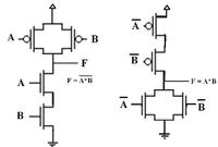
I don’t completely understand the above explanation when I think that it is possible to design noninverting gates using STATIC CMOS Logic (for instance, the AND gate as shown in figure 1).
1- What is the message behind the above sentence?
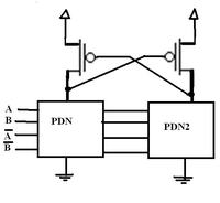
2- In addition, what is the advantage of DCVSL (Differential Cascode Voltage Switch logic) compared to the traditional Static logic? why? Please, see figure 2.
Thank you very much,
Regards,
Please, could you clarify me the following confusion regarding Static CMOS logic?
In the Rabaey book, it is said that "Static CMOS gate is naturally inverting and the realization of a noninverting Boolean function (such as AND , OR, XOR) in a single stage is not possible."
I don’t completely understand the above explanation when I think that it is possible to design noninverting gates using STATIC CMOS Logic (for instance, the AND gate as shown in figure 1).
1- What is the message behind the above sentence?
2- In addition, what is the advantage of DCVSL (Differential Cascode Voltage Switch logic) compared to the traditional Static logic? why? Please, see figure 2.
Thank you very much,
Regards,

