Continue to Site

Welcome to EDAboard.com

Welcome to our site! EDAboard.com is an international Electronics Discussion Forum focused on EDA software, circuits, schematics, books, theory, papers, asic, pld, 8051, DSP, Network, RF, Analog Design, PCB, Service Manuals... and a whole lot more! To participate you need to register. Registration is free. Click here to register now.

SIlvaco TCAD PIN Photodiode

Status
Not open for further replies.

ida89

Newbie level 4
Newbie level 4
Joined
Mar 6, 2013
Messages
6
Helped
0
Reputation
0
Reaction score
0
Trophy points
1,281
Visit site
Activity points
1,317
hye, i want to ask, can i create a structure of PIN photodiode in reverse arrangenment? from P-I-N to N-I-P. thanks
 

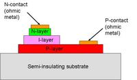
Not sure but, CdTe cells use NIP structure, a variation of the PIN structure. In a NIP structure, an intrinsic CdTe layer is sandwiched by n-doped CdS and p-doped ZnTe. The photons are incident on the n-doped layer unlike a PIN diode. Somewhat like this:
 

Status
Not open for further replies.

Part and Inventory Search

Welcome to EDABoard.com

Sponsor

Back
Top