Continue to Site

Welcome to EDAboard.com

Welcome to our site! EDAboard.com is an international Electronics Discussion Forum focused on EDA software, circuits, schematics, books, theory, papers, asic, pld, 8051, DSP, Network, RF, Analog Design, PCB, Service Manuals... and a whole lot more! To participate you need to register. Registration is free. Click here to register now.

should i use RF mos to avoid body effect?

Status
Not open for further replies.

sw0ws1

Junior Member level 1
Joined
Jul 15, 2010
Messages
19
Helped
2
Reputation
4
Reaction score
1
Trophy points
1,283
Activity points
1,428
hi
i use 0.18UM180FDKMFC-FDK
in my design i have to avoid body effect so i need to connect the bulk terminal of NMOS to its source
but the problem is the process is twin well
so can i use RF mos in the kit?it has 4 terminals (s,D,G ,B) , when i see RF transistor layout it has a layer called DNW ,does it mean "deep n well"??? and if so can i connect the bulk to source now??

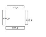
the following figure appears when i make the layer DNW is the only visible in the layout of transistor
salwa.png
thanks in advance
 
Last edited:

The answer seems to be yes.Take a look at this thread,it will help you and make you understand the usage of DNW (deep n-well) layer :

https://www.edaboard.com/threads/85902/

In any case,for such questions always be consulted by your technology documentation.
 

hi
i use 0.18UM180FDKMFC-FDK
in my design i have to avoid body effect so i need to connect the bulk terminal of NMOS to its source
but the problem is the process is twin well
so can i use RF mos in the kit?it has 4 terminals (s,D,G ,B) , when i see RF transistor layout it has a layer called DNW ,does it mean "deep n well"??? and if so can i connect the bulk to source now??

the following figure appears when i make the layer DNW is the only visible in the layout of transistor
View attachment 56818
thanks in advance

It seems you are using some variant of UMC .18; I have used one of their kits before but I've never seen a pcell for DNW NFETs even though I know the option is available

In any case using an RF device or a std device is irrelevant as long as you respect the rules for DNW

Just beware of using DNW devices with only 4 terminals, I strongly recommend that you find a way to extract the other two terminals e.g. by adding the parasitic diodes and checking the LVS rules if there is an option to activate that check

As of your figure, the usage of DNW depends on the kit but in general DNW should be a shape over the whole device enclosed by an NW ring to bias the buried DNW layer and create the isolated PW (sometimes called RW)
 

Yes you can use it but you should understand what RF MOS really is. Usually it means that it is fix W/L device with and characterized just for this size.
If you need 4 terminal mosfet you can use just any device in deepNwell. - the problem will be if the LVS and DRC recognizes this device - but it should.
Spice model would be same as for any other MOS on the chip.
 

It depends on what cost you want to pay for it. If you use additional RF device, additional masks are needed. And wafer cost is higher.
 

It depends on what cost you want to pay for it. If you use additional RF device, additional masks are needed. And wafer cost is higher.
Additional masks for RF FETs? That does not ring a bell and we have submitted a fair number of designs using different RF processes, I have never seen masks specific to RF FETs, can you provide an example?
 

Status
Not open for further replies.

Part and Inventory Search

Welcome to EDABoard.com

Sponsor

Back
Top