Continue to Site

Welcome to EDAboard.com

Welcome to our site! EDAboard.com is an international Electronics Discussion Forum focused on EDA software, circuits, schematics, books, theory, papers, asic, pld, 8051, DSP, Network, RF, Analog Design, PCB, Service Manuals... and a whole lot more! To participate you need to register. Registration is free. Click here to register now.

Series/parallel charge pump

Status
Not open for further replies.

Mira7

Newbie level 4
Joined
Jul 28, 2013
Messages
7
Helped
0
Reputation
0
Reaction score
0
Trophy points
1
Activity points
69
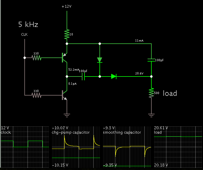
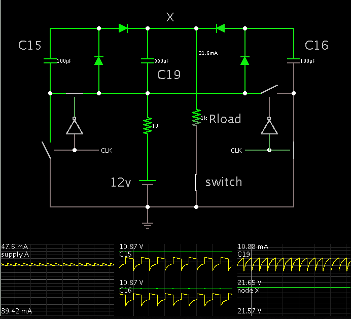
I am designing a series/parallel charge pump, which is a kind of DC-DC-converter. However it does not operate as I intended. Can you spot an error in the design?

Circuit: View attachment Charge pump.pdf
 

why are so many base terminals un-connected?
 

why are so many base terminals un-connected?

Each gate is connected to an IGBT gate driver IC powered by a separate isolated DC-DC-converter. All (5) gate signals are generated by an Arduino and pre-amplified before being sent to their respective gate driver IC. This part is verified to operate as expected. The state changes are described in the PDF.
 

Each gate is connected to an IGBT gate driver IC powered by a separate isolated DC-DC-converter. All (5) gate signals are generated by an Arduino and pre-amplified before being sent to their respective gate driver IC. This part is verified to operate as expected. The state changes are described in the PDF.

That makes it more clear. You have FIVE DC-DC converters? It seems quite elaborate and overly engineered. Is there a reason why you attempted this approach?
 

Reduce R10, to, say 10 ohms. The circuit needs to draw large current spikes during the first few cycles, to get off the ground.

You can eliminate D15.

You need to put a diode in series with the load.

C19 needs to be positioned so it goes from the supply to the top of the load.

Here is the simplest charge-pump doubler I am familiar with:


It will resemble your design, if you make the above changes.

Also, the right half (rightmost 3 components) of your circuit interferes with operation of the left half. You'll need to install two more diodes in order to make the two charge pumps work together in interleaved fashion. (This will make a total of 4 diodes.)
 

BradtheRad, thanks. I have updated the schematics. it is unclear to me how you suggested to connect C19. I have added the description section to the attached PDF explaining the switch states and the intended use of C19 as an energy recovery capacitor. it is unclear to me where to put the two extra diodes you suggested for separation. the left side should charge the capacitor on the right side and vice versa, so they should not be separated. what is needed to discharge correctly, recover the undissipated energy, and re-use it in the next charge cycles?

new PDF attached.
 

Attachments

  • Charge pump.pdf
    77.8 KB · Views: 71

BradtheRad, thanks. I have updated the schematics. it is unclear to me how you suggested to connect C19. I have added the description section to the attached PDF explaining the switch states and the intended use of C19 as an energy recovery capacitor. it is unclear to me where to put the two extra diodes you suggested for separation. the left side should charge the capacitor on the right side and vice versa, so they should not be separated. what is needed to discharge correctly, recover the undissipated energy, and re-use it in the next charge cycles?

new PDF attached.

You connected C19 correctly.

Here is a simulation of your twin interleaved charge-pump voltage doubler. (Using Falstad's simulator).


It works on a different concept from that of charging capacitors in parallel, then discharging them in series.
 

You connected C19 correctly.

Here is a simulation of your twin interleaved charge-pump voltage doubler.

I acknowledge that in your suggested circuit, the supply voltage is doubled. however I am not trying to double the supply voltage. I am trying to design an efficient DC charge pump that converts a fairly low voltage, say 12V, into a much higher voltage, say 200V for now, without using (inefficient) inductors.
then by quickly expanding the capacitance of the circuit, a large current can be made to flow through a low resistance load according to E=1/2*C*V*V. it should be possible to re-use part of the undissipated energy in the following charge cycles. what changes need to be made to accomplish this?
 

I believe you are describing a 17x voltage multiplier.

Depending on which type of building block you decide to use, you'll need a few dozen charge pump cells, to reach 200V.

One type of building block is the Villard cell, consisting of a diode/capacitor pair. Each stage subtracts 0.6V by way of a diode drop. To make up for the loss, you'll need to add an extra Villard stage or two.

(There could be an alternate topology, consisting of an arrangement of myriad switching devices, which avoids such voltage drops. Example, Nakagome charge pump.)

There is also the question whether you want to turn 12VDC into pulsed DC, or into AC by means of a full H-bridge.

Here is a simulation to illustrate how 9VDC could go through 8 Villard stages to become 34VDC.


I believe you are describing a 17x voltage multiplier.

the output voltage should not be a fixed multiple of the input voltage determined by the hardware, but rather determined by the number of charge cycles controlled by an Arduino microcontroller. so say I want 400V output instead of 200V output, I just put two 250V 100uF capacitors in series configuration at each side of the circuit (see first attached PDF) and change the Arduino software to double the number of charge cycles between each discharge.

the discharge is also controlled by the Arduino so pulsed DC is sent through the resistive load.

I described the behavior of and problems with my initial circuit in the first attached PDF. I do feel like it does not need many changes to get a working solution. it may just be something trivial that I am not able to see due to lack of experience with electronics.

can anyone see what changes are needed?
 

Now I think I get what you want to do:

Charge the first capacitor to 12V...

then re-orient it (via switching devices) so its charge is added to the supply V...

to charge the second capacitor.

Then re-orient the second capacitor, to add its elevated charge to the supply V...

and charge the first capacitor to an even higher volt level.

----------------

This can work theoretically. However it will require more switching devices (transistors, mosfets, etc.) I have not seen any circuit design which does this.

It will probably require non-polarized capacitors.

There is the obstacle because of how transistors and mosfets work. For a transistor to turn on, the base current needs to have a complete return path going from the emitter leg around the loop. This can create a problem when there are multiple transistors in series.
Similarly, a mosfet needs to see a definite volt level at whichever terminal the gate is referenced to. Unreliable operation can result, when you have multiple devices in series.

The switching devices shown in my post #7 schematic are theoretical. Only one wire is needed to turn them on and off. This makes it easy for us to experiment with unusual circuit designs. However I have not seen such a switching component in the real world.

The closest thing might be a 4066 IC (bilateral analog switch, 4 of them on a chip). But you may find that the 'On' resistance is be too high to permit enough current flow. There ought to be a similar device which has a lower 'On' resistance.
 

you described correctly what I am trying to achieve. The initial design uses IGBTs which are voltage-controlled rather than current-controlled like BJTs. ideally no current flows into the base of the IGBTs.

non-polarized capacitors is not a problem to do since it can be created with two polarized capacitors in series. I just currently do not see the need for that. maybe you can enlighten me?

we also need to keep in mind that IGBTs are unidirectional. did you suggest that there is a problem due to two IGBTs being connected in series? that they interfere with eachother? I remind that each IGBT gate drive IC is grounded to its respective IGBT emitter and have isolated power sources.

thank you for your assistance.
 

I tried to extract a concept from the descriptions in posts #1 and #6, but I wasn't able to. Up to now, it looks to me just like an error of reasoning.

With two capcitors switched between series and parallel circuit, you can maximally achieve voltage doubling, but nothing beyond.

Before discussing real switch behaviour and control, you should explain the basic concept, using ideal switches (with finite resistance, however). Everything can be calculated in terms of charge and energy.
 

With two capcitors switched between series and parallel circuit, you can maximally achieve voltage doubling, but nothing beyond.

I agree. however I do many swaps (10 or 20) and the external energy source (lab power supply) can supply energy continuously during device operation.

- - - Updated - - -

I just had the thought that C15 will much rather supply energy to C16 than V9 due to the much smaller resistance.

that will then reduce the potential difference between V9/C15 and C16 relatively quickly and thereby prevent V9 from delivering energy to C16.

one could then just insert a relatively large resistance between C15 and C16, but that would be inefficient.

ideally I just want C15 to supply only potential, but no energy to C16 so that all energy to C16 is supplied by V9. does anyone have any suggestions as to how this can be accomplished?

this does however not explain the increased current (approx. 100mA) I observe at each swap.
 

Status
Not open for further replies.

Part and Inventory Search

Welcome to EDABoard.com

Sponsor

Back
Top