Continue to Site

Welcome to EDAboard.com

Welcome to our site! EDAboard.com is an international Electronics Discussion Forum focused on EDA software, circuits, schematics, books, theory, papers, asic, pld, 8051, DSP, Network, RF, Analog Design, PCB, Service Manuals... and a whole lot more! To participate you need to register. Registration is free. Click here to register now.

SEPIC with voltage error amplifier is more easy to make stable..why?

Status
Not open for further replies.
T

treez

Guest
Hello,
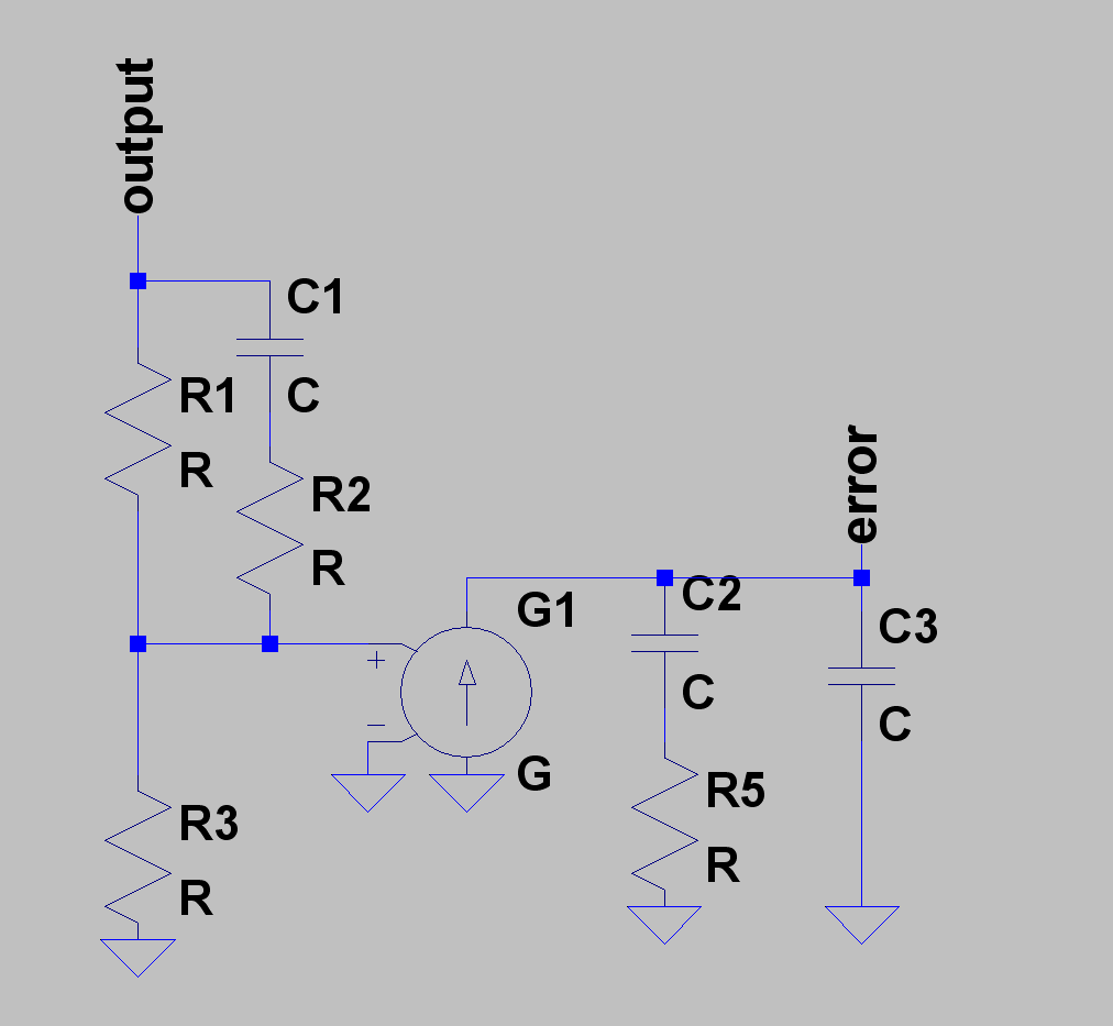
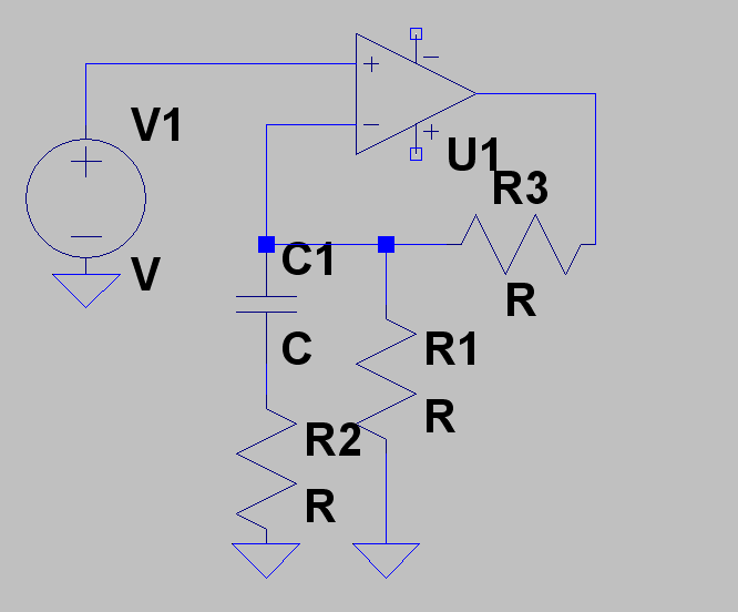
Here are two identical 20W SEPIC LED drivers that use the LTC1871 PWM controller. (Vin=12V, Vout=~45V, Fsw=90KHz, Current mode)

One connects the error amplifier in "voltage error amplifier" configuration.
The other connects the error amplifier in the "transconductance error amplifier" configuration.

The one with the "voltage error amplifier" configuration is far easier to stabilise.
The "transconductance error amplifier" configuration version has to be given an extremely slow transient response in order to make it stable.

Why does the LTC1871 datasheet not recommend the "voltage error amplifier" configuration connection?
It doesn't seem to make sense.

LTC1871 datasheet:
http://cds.linear.com/docs/en/datasheet/1871fe.pdf

Schematics are below...also the LTspice simulations
 

Attachments

  • SEPIC voltage error amp.pdf
    34.1 KB · Views: 103
  • SEPIC transconductance error amp.pdf
    32.9 KB · Views: 96
  • SEPIC voltage error amp.txt
    8.1 KB · Views: 45
  • SEPIC transconductance error amp.txt
    7.9 KB · Views: 54

It all comes down to where the zeros and poles are. The circuit implementation is just a detail, and there are many ways to implement a given frequency response. There's no reason either circuit can't give the same quality of results.
 
  • Like
Reactions: treez

    T

    Points: 2
    Helpful Answer Positive Rating
if one trys the simulations, its clear that getting the same speed of start up is far far harder with the transconductance error amplifier.
I am not sure what the maximum output current of the transconductance amp is though, and so if the resistor R11 was too low value, then I think the transconductance amp would have difficulty in supplying enough current when connected in voltage configuration?
Unfortunately the datasheet doesn't say either the output impedance of the transconductance amp, or what is its maximum source/sink current capability.

Just hacking the above simulations, it seems obvious that transconductance style error amplifiers are a mistake with led drivers.....that resistor R11 is needed with leds, as the led load is effectively the upper feedback divider resistor, and it has low dynamc resistance, so R11 is needed , but cant be put there when a transconductance style error amplifier is used.
 

if one trys the simulations, its clear that getting the same speed of start up is far far harder with the transconductance error amplifier.
I ran the simulations, and the one with the standard transconductance amp starts up slow and smooth, and the "voltage" ramps up faster but overshoots tremendously and is very underdamped. Obviously some sort of nonlinear action is taking place as well (and changing Vin around affects this a lot). Between the two, the voltage mode one has unacceptable response, rise time be damned.
I am not sure what the maximum output current of the transconductance amp is though, and so if the resistor R11 was too low value, then I think the transconductance amp would have difficulty in supplying enough current when connected in voltage configuration?
Unfortunately the datasheet doesn't say either the output impedance of the transconductance amp, or what is its maximum source/sink current capability.
The amplifier current limit could be an issue. I see it never swinging past +/-40uA in my simulations. But if that's the case you just increase the impedance of the output network and lower the gain of the external amplifier you have their.

Just hacking the above simulations, it seems obvious that transconductance style error amplifiers are a mistake with led drivers.....that resistor R11 is needed with leds, as the led load is effectively the upper feedback divider resistor, and it has low dynamc resistance, so R11 is needed , but cant be put there when a transconductance style error amplifier is used.
Why would you make such a sweeping generalization based on "hacking" some simulations?? Did you do any analysis beyond trial and error? If not then you should probably just stick to the equations and circuits in the datasheet.
 
  • Like
Reactions: treez

    T

    Points: 2
    Helpful Answer Positive Rating
Between the two, the voltage mode one has unacceptable response

The point is that the "voltage" one can much , much more easily be made much faster than the "transconductance" one.

Yes I do have that overshoot, but I can quell that with a bit of component changes.....in any case, that overshoot in the led current is only for 100us or so and will not damage the leds.
It is simply not possible to get any kind of fast transient response out of the "transcondutance" one...as it goes unstable, which indicates that it has poorer gain and phase margin.

As far as calculations go.....I would do a calculation, but to be honest , we will just put in an injection resistor and confirm good gain and phase marging with a frequency analyser , as it only takes 30 seconds to get a reading..........

With led drivers., as you know.....the response isn't that important, its just important to get stability, and since the "voltage" type is more stable, we would pick that every time.

I never calculate feedback components for led drivers to start off with.......we just do them by geek hacking, and then confirm with the frequency analyser.......we then do do the calculation, and check it corresponds to the frequency analyser......as you know, the frequency analyser plot is "king".

Feedback compensation calculations are great, but seriously, what is the exact esr of say a ceramic capacitor? (as you know, this is one of the compensation design values)......there's so much tolerance on it, we'd rather just get out the gain phase analyser.
Also, with things like a sepic, how does the rc snubber across the sepic cap affect the gain/phase margin?....also how does the loosely tolerant leakage in the sepic inductor, if used, affect the compensation math?........its just quicker to "geek hack" it then measure it with the AP300.
 

The point is that the "voltage" one can much , much more easily be made much faster than the "transconductance" one.

It is simply not possible to get any kind of fast transient response out of the "transcondutance" one...as it goes unstable, which indicates that it has poorer gain and phase margin.
Prove it. Hint: doing a bunch of trial and error simulations does not constitute proof.

As far as calculations go.....I would do a calculation, but to be honest , we will just put in an injection resistor and confirm good gain and phase marging with a frequency analyser , as it only takes 30 seconds to get a reading..........

With led drivers., as you know.....the response isn't that important, its just important to get stability, and since the "voltage" type is more stable, we would pick that every time.
Just by looking at the transient response it's clear that the voltage type one is far less stable. It nearly oscillates if the input voltage is set to 9V. The transconductance one has no such problems.

I never calculate feedback components for led drivers to start off with.......we just do them by geek hacking, and then confirm with the frequency analyser.......we then do do the calculation, and check it corresponds to the frequency analyser......as you know, the frequency analyser plot is "king".
A measurement can tell you if the thing meets spec or not. It can't tell you things like
getting the same speed of start up is far far harder with the transconductance error amplifier
or
transconductance style error amplifiers are a mistake with led drivers
Only in depth analysis can justify such categorical claims.
Feedback compensation calculations are great, but seriously, what is the exact esr of say a ceramic capacitor? (as you know, this is one of the compensation design values)......there's so much tolerance on it, we'd rather just get out the gain phase analyser.
Also, with things like a sepic, how does the rc snubber across the sepic cap affect the gain/phase margin?....also how does the loosely tolerant leakage in the sepic inductor, if used, affect the compensation math?........its just quicker to "geek hack" it then measure it with the AP300.
Honestly, how much effort have you actually put into answering these questions yourself, rather than relying on "geek hacks" and rules of thumb? It's fine if you rely on them for your own designs, and share them with others, but you should know that those useful "hacks" mostly didn't arise from people playing with simulations, they came from rigorous analysis and verification. And I have a problem with people coming up with their own tricks and spreading them around engineering communities, despite those "tricks" only being tested by trial and error in a few simulations in a single application.
 

I take your good points, though I am trying to do a pressman type 3 type of feedback, where I can get good stability and fast rise up into regulation.......the way of doing it with the transconductance error amplifier is more convoluted as I find here....LTspice sims and schems attached.

I am not sure how to do a pressman type 3 with a transconductance error amplifier, not sure of it is possible.?
 

Attachments

  • SEPIC 90K Transconductance_1.pdf
    34.1 KB · Views: 90
  • SEPIC 90K voltage error amp_1.pdf
    34 KB · Views: 96
  • SEPIC 90K voltage error amp_1.txt
    8.5 KB · Views: 128
  • SEPIC 90K Transconductance error amp_1.txt
    8.8 KB · Views: 42
Last edited by a moderator:

The network in the standard transconductance amp by itself is just a type II network (two poles, one zero). This is typically sufficient for current mode supplies. If you want another pole zero pair to get a type 3 response, then it can be done with an additional RC network between the output and the FB pin. Like this:

This is actually simpler because the poles and zeros defined by each network are independent, unlike when you have one of the networks feed back to the FB pin. The locations of the poles and zeros are therefore easier to calculate, and component values are easier to choose.

One potential problem with your design: I assume you are using that extra amplifier so that you can use a lower value current sense resistor for the output. This is a fine idea, but this gain will also affect the AC response of course, meaning you will have to lower the impedance of the network on the transconductance amp's output (in order to get the AC gain back down). This means that the current limit of the transconductance amplifier may come into play more, and if it does it may cause the startup time of the whole circuit to be slower. However you must know that this does not necessarily indicate anything about the stability or bandwidth of the feedback loop once it's reached a steady state.
 

yes youre right its because I wish the lower value sense resistor.
The upper "R" in your diagram is the upper divider resistor in a voltage regulated smps......as you know, with led drivers, that upper "R" is the blessed LEDs......and they of course have very low dynamic resistance....I don't know if that effects things?....

I see your point about the separate networks being advantageous..though..

The following is like a compromise between "transconductance" and "voltage" error amps, and I wonder if this is an idea.
 

Attachments

  • SEPIC 90K Transconduc_2.pdf
    33.7 KB · Views: 80
  • SEPIC 90K Transconductance error amp_2.txt
    8.5 KB · Views: 41

Correct, that method relies on attenuation. Here's an alternate method to implement the extra pole/zero pair in your external amplifier stage:

A very simple modification.
 

Sorry Mtwieg I don't now see your attachments?
However, I took it that you yourself believe that any of the three error amplifier connections offered above are perfectly valid?

ie
1...Voltage error amplifier connection
2...Transconductance error amplifier connection
3...Mixture of both of the above.
 

It all comes down to where the zeros and poles are. The circuit implementation is just a detail, and there are many ways to implement a given frequency response. There's no reason either circuit can't give the same quality of results.
There's not much more to say, unless you have a more specific question.
 
  • Like
Reactions: treez

    T

    Points: 2
    Helpful Answer Positive Rating
thanks, though I cannot understand why they even suggest the transconductance error amplifier configuration, when it is more limited in terms of not being easily able to do a type 3 compensation with LED loads? (though I do take your point about the separation of the bits) (I might not always have the external amplifier)........but it looks like I can use your "RC to ground" method even without an external amplifier?
Are you sure your subcircuit of post #10 gives a type 3?...I thought type 3 was like "feedforward" from the output rail, like in your #8?...like in the attached for leds...(R14, C10, R12 give the type 3?)
 

Attachments

  • SEPIC voltage error amp_1.pdf
    34.6 KB · Views: 95
Last edited by a moderator:

thanks, though I cannot understand why they even suggest the transconductance error amplifier configuration, when it is more limited in terms of not being easily able to do a type 3 compensation with LED loads? (though I do take your point about the separation of the bits) (I might not always have the external amplifier)........
Yes, with the error amplifier alone you typically just implement a type II network (two poles, one zero). To make it a type III you build a RC network into the feedback attenuator. As you point out, this is not easy with a LED driver, since attenuation in the current sense signal is no good (unless you use another external amplifier). In a very practical sense, this makes type III compensation a little more of a hassle to achieve with a current regulate supplies using tranconductance amps.

Are you sure your subcircuit of post #10 gives a type 3?...I thought type 3 was like "feedforward" from the output rail, like in your #8?...like in the attached for leds...(R14, C10, R12 give the type 3?)
#10 shows just how to add an extra pole/zero pair to an external amplifier in order to make a type II into a type III, as explained above.

But keep in mind that if you're using a current mode controller, type III compensation is almost never necessary.
 
  • Like
Reactions: treez

    T

    Points: 2
    Helpful Answer Positive Rating
But keep in mind that if you're using a current mode controller, type III compensation is almost never necessary.
..even in the case of a Continuous current mode SEPIC?
 

Yes. For current mode converters operating in CCM, you have one dominant pole in the transfer function. Depending on the converter type, there will be more poles or RHP zeros at higher frequencies, but those will always become a bottleneck on your fc, even if you use type III compensation. Going from type II to type III can only get up to 90 degrees of extra phase boost, but that's not enough to overcome the effect of a RHP zero or a pair of conjugate poles.
 
  • Like
Reactions: treez

    T

    Points: 2
    Helpful Answer Positive Rating
..but type 3 might be enough to overcome start-up overshoot in vout, or overshoot in vout following recovery from short circuit output?
 

Status
Not open for further replies.

Part and Inventory Search

Welcome to EDABoard.com

Sponsor

Back
Top